The article explores various aspects of reverse-biased diode, including transient current behavior, reverse saturation current, differences between silicon and germanium diodes, and surface-leakage current. It discusses how these factors impact the performance and applications of diodes in electronic circuits.
Let’s discuss a few advanced ideas about a reverse-biased diode. To begin with, the depletion layer changes in width when the reverse voltage changes. Let us see what this implies.
Transient Current
When the reverse voltage increases, holes and electrons move away from the junction. As the free electrons and holes move away from the junction, they leave positive and negative ions behind. Therefore, the depletion layer gets wider. The greater the reverse bias, the wider the depletion layer becomes. While the depletion layer is adjusting to its new width, a current flows in the external circuit. This transient current drops to zero after the depletion layer stops growing.
The amount of time the transient current flows depends on the RC time constant of the external circuit. It typically happens in a matter of nanoseconds. Because of this, you can ignore the effects of the transient current below approximately 10 MHz.
Reverse Saturation Current
Forward-biasing a diode decreases the width of the depletion layer and allows free electrons to cross the junction. Reverse bias has the opposite effect: It widens the depletion layer by moving holes and free electrons away from the junction.
Suppose that thermal energy creates a hole and free electron inside the depletion layer of a reverse-biased diode, as shown in Figure 1. The free electron at A and the hole at B can now contribute to reverse current. Because of the reverse bias, the free electron will move to the right, effectively pushing an electron out of the right end of the diode. Similarly, the hole will move to the left. This extra hole on the p side lets an electron enter the left end of the crystal.
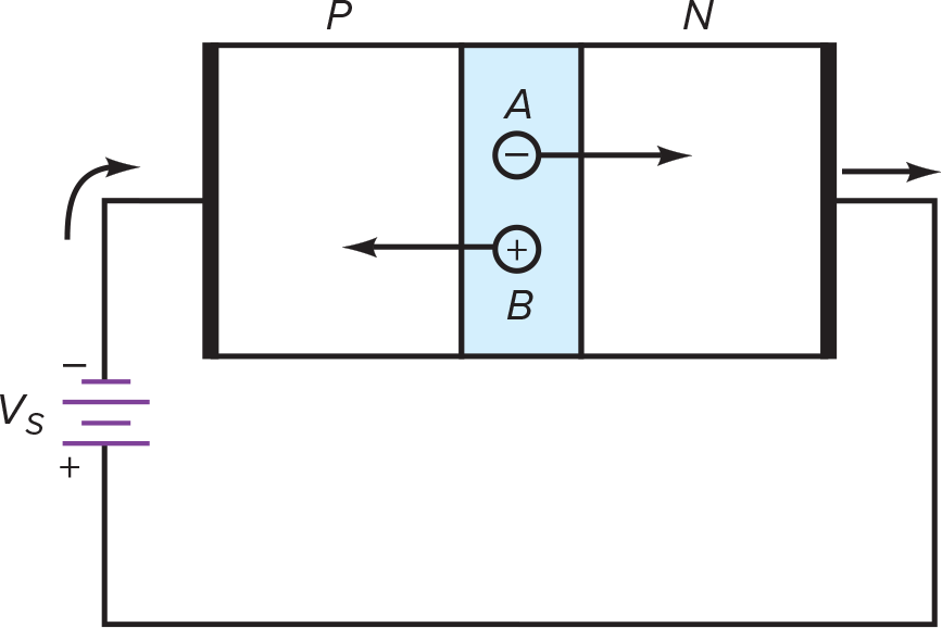
Figure 1. Thermal energy produces free electron and hole inside depletion layer.
The higher the junction temperature, the greater the saturation current. A useful approximation to remember is this: IS doubles for each 10°C rise. As a derivation,
$$Percent\ \Delta I_S=100%\ for\ a\ 10°C increase$$
In words, the change in saturation current is 100 percent for each 10°C rise in temperature.
If the changes in temperature are less than 10°C, you can use this equivalent rule:
$$Percent\ \Delta I_S=7%\ per\ °C$$
In words, the change in saturation current is 7 percent for each Celsius degree rise. This 7 percent solution is a close approximation of the 10° rule.
Silicon versus Germanium
In a silicon atom, the distance between the valence band and the conduction band is called the energy gap. When thermal energy produces free electrons and holes, it has to give the valence electrons enough energy to jump into the conduction band. The larger the energy gap, the more difficult it is for thermal energy to produce electron-hole pairs. Fortunately, silicon has a large energy gap; this means that thermal energy does not produce many electron-hole pairs at normal temperatures.
In a germanium atom, the valence band is much closer to the conduction band. In other words, germanium has a much smaller energy gap than silicon has. For this reason, thermal energy produces many more electron-hole pairs in germanium devices. This is the fatal flaw mentioned earlier. The excessive reverse current of germanium devices precludes their widespread use in modern computers, consumer electronics, and communications circuits.
Just as silicon semiconductors have replaced most germanium devices, new developments in the semiconductor manufacturing industry are occurring where compound semiconductors made from silicon carbide SiC and gallium nitride GaN are being produced to replace standard silicon devices. These new semiconductors are referred to as wide band gap (WBG) devices and have enhanced properties, such as higher electron mobility, reduced leakage currents, and higher breakdown voltages.
What is a Surface-Leakage Current?
Surface-leakage current is a reverse current on the surface of the crystal. Here is an explanation of why surface-leakage current exists.
Suppose that the atoms at the top and bottom of Figure 2a are on the surface of the crystal. Since these atoms have no neighbors, they have only six electrons in the valence orbit, implying two holes in each surface atom. Visualize these holes along the surface of the crystal shown in Figure 2b. Then you can see that the skin of a crystal is like a p-type semiconductor. Because of this, electrons can enter the left end of the crystal, travel through the surface holes, and leave the right end of the crystal. In this way, we get a small reverse current along the surface.
Figure 2. (a) Atoms on the surface of a crystal have no neighbors
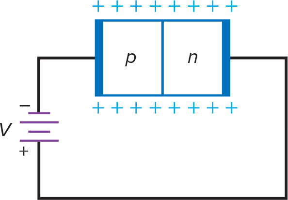
Figure 2. (b) surface of crystal has holes.
The surface-leakage current is directly proportional to the reverse voltage. For instance, if you double the reverse voltage, the surface-leakage current ISL doubles. We can define the surface-leakage resistance as follows:
$$R_{SL}=\frac{V_R}{I_{SL}}$$
Surface Leakage Current Example
If the surface-leakage current is 2 nA for a reverse voltage of 25 V, what is the surface-leakage current for a reverse voltage of 35 V?
Solution
There are two ways to solve this problem. First, calculate the surface-leakage resistance:
$$R_{SL}=\frac{25V}{2\ nA}=12.5\left({10}^9\right)\ \Omega$$
Then calculate the surface-leakage current at 35 V as follows:
$$I_{SL}=\frac{35V}{12.5\left({10}^9\right)\ \Omega}=2.8\ nA$$
Here is a second method. Since surface-leakage current is directly proportional to reverse voltage:
Reverse-Biased Diode Key Takeaways
Understanding the behavior of reverse-biased diodes is crucial for various applications in electronics. Transient current and reverse saturation current affect the stability and performance of diode circuits, while the choice between silicon and germanium diodes influences their efficiency and reliability. Furthermore, surface-leakage current plays a significant role in high-voltage applications, where even small currents can have significant effects.