The article provides an overview of transistor amplifier, covering the theory and function of amplification, types of transistor amplifier circuits, transistor biasing, and current flow mechanisms. It also discusses amplifier gain, transistor configurations (PNP and NPN), and outlines standard packaging and symbol representations.
Amplification is the process of taking a small signal and making it larger. In control systems, amplifiers are used to increase small signal currents and voltages so they can do useful work.
Amplification is accomplished by using a small input signal to control the energy output from a larger source such as a power supply.
Amplification is accomplished by transistors and operational amplifiers (op-amps). Amplifiers are essential for increasing the effect of a small change in voltage. Current and resistance are produced by input sensors.
Amplifier Gain
The primary objective of an amplifier is to produce gain. Gain is a ratio of the amplitude of an output signal to the amplitude of an input signal.
In determining gain, the amplifier can be thought of as a black box. A signal applied to the input of the black box results in an output from the box. Mathematically, the gain can be found by dividing output by input:
\[Gain=\frac{Output}{Input}\]
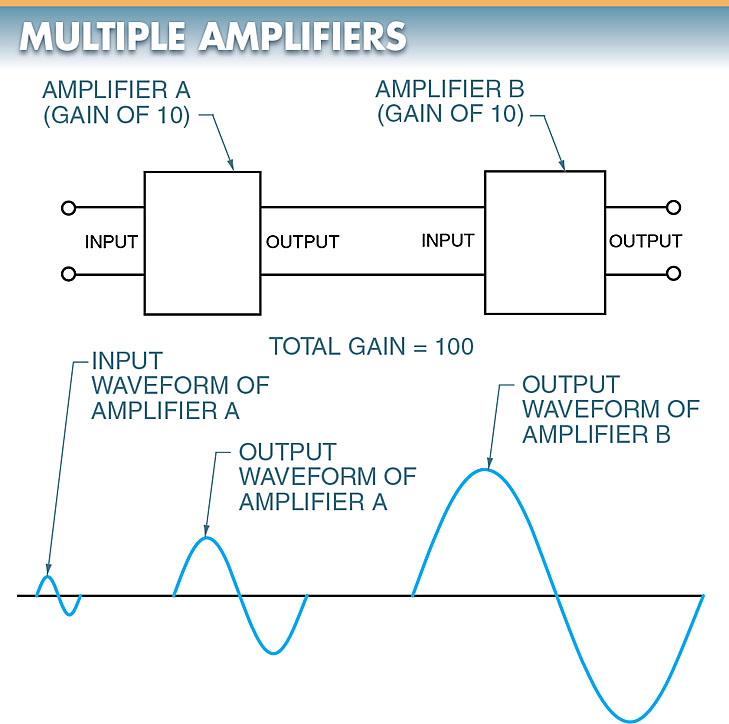
Often, a single amplifier does not provide enough gain to increase the output signal to the amplitude needed. In such a case, two or more amplifiers can be used to obtain the gain required. See Figure 1.
For example, amplifier A has a gain of 10 and amplifier B has a gain of 10. The total gain of the two amplifiers is 100 (10 × 10 = 100). If the gains of the amplifiers were 8 and 9, respectively, the total gain would be 72 (8 × 9 = 72).
Amplifiers connected in this manner are called cascaded amplifiers. For many amplifiers, the gain is in the hundreds or even thousands.
Figure 1. Adding amplifiers to obtain the required gain if a single amplifier does not provide enough gain to increase the output signal to the amplitude needed.
Note: Gain is a ratio of output to input and has no unit of measure, such as volts or amps, attached to it. Therefore, the term gain is used to describe current gain, voltage gain, and power gain. In each case, the output is merely being compared to the input.
Transistor Amplifier Theory
Transistors may be used as AC amplification devices. A transistor is a three-terminal device that controls the current through the device depending on the amount of voltage applied to the base. Transistors are bipolar devices.
A bipolar device is a device in which both holes and electrons are used as internal carriers for maintaining current flow. Transistors may be PNP or NPN transistors.
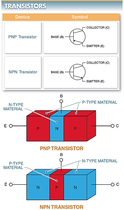
A PNP transistor is formed by sandwiching a thin layer of N-type material between two layers of P-type material. An NPN transistor is formed by sandwiching a thin layer of P-type material between two layers of N-type material. See Figure 2.
Figure 2. PNP transistor symbol & NPN transistor symbol
Transistor terminals are the emitter (E), base (B), and collector (C). The symbols for PNP and NPN transistors show the emitter, base, and collector in the same places. The difference in the terminals is the direction in which the emitter arrow points.
In both cases, the arrow points from the P-type material toward the N-type material.
Transistor Amplifier Circuit Diagram
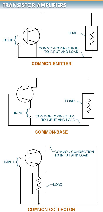
The three basic transistor amplifiers are the common-emitter, common-base, and common-collector. See Figure 3.
Each amplifier is named after the transistor connection that is common to both the input and the load. For example, the input of a common-emitter circuit is across the base and emitter, while the load is across the collector and emitter. Thus, the emitter is common to the input and load.
Figure 3. The three basic transistor amplifiers circuit diagram: common-emitter transistor amplifier, common-base transistor amplifier, and common-collector transistor amplifier.
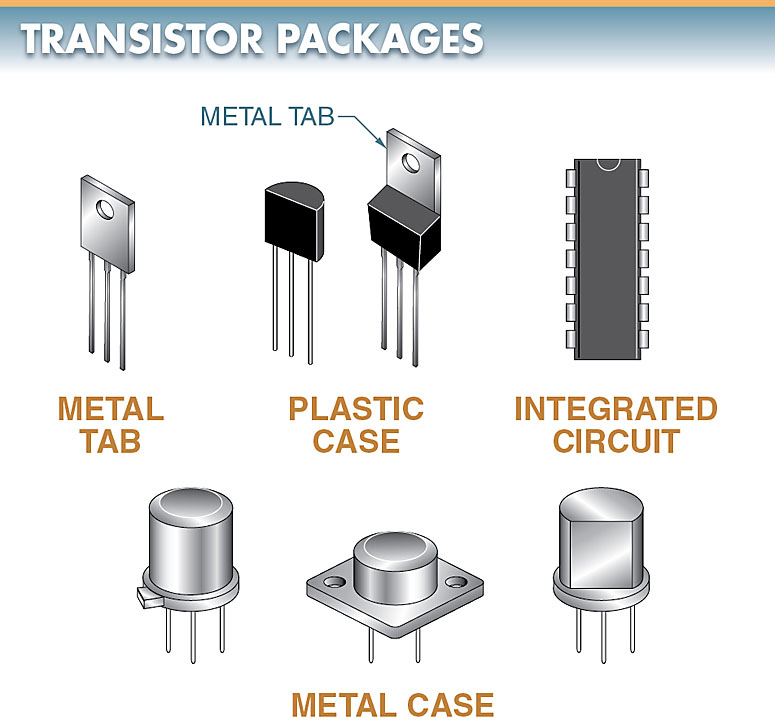
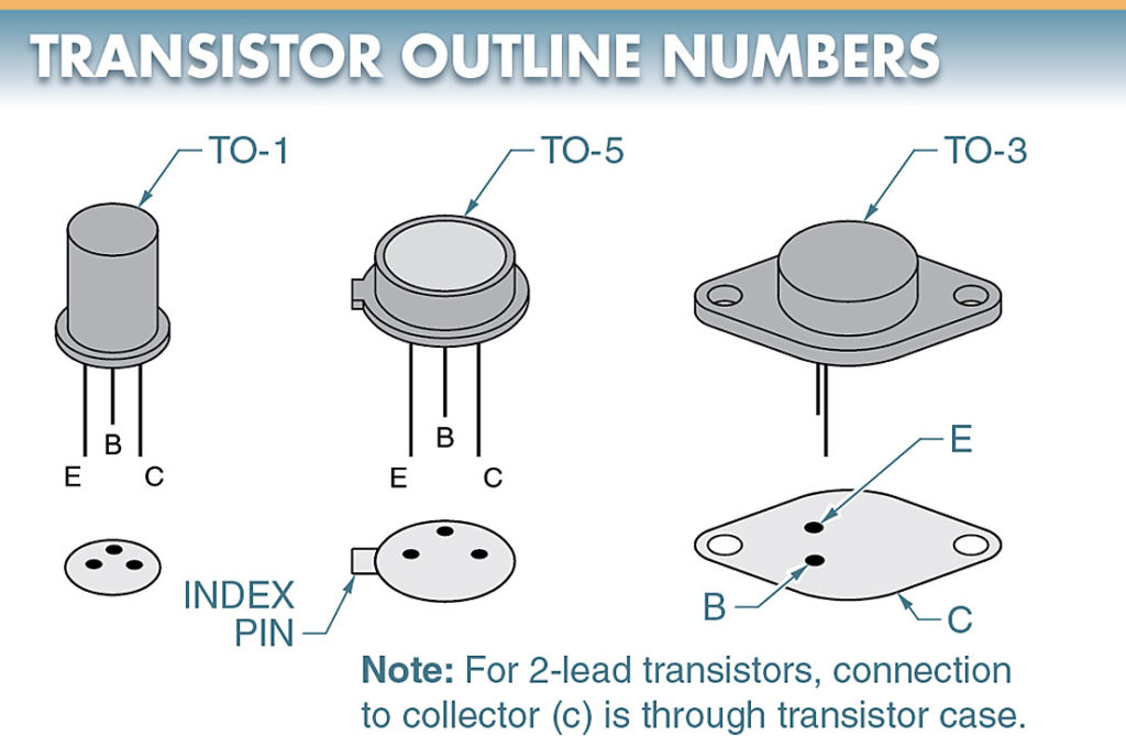
Transistors are manufactured with two or three leads extending from their case. See Figure 4. These packages are accepted industry-wide regardless of manufacturer.
When a transistor with a specific shape must be used, a transistor outline (TO) number is used for reference.
A transistor outline (TO) number is a number determined by the manufacturer that represents the shape and configuration of a transistor. See Figure 5.
Transistor outline numbers are determined by individual manufacturers. Note: The bottom view of transistor TO-3 shows only two leads (terminals). Typically, transistors use the metal case as the collector-pin lead.
Figure 4. Transistors have either two or three leads extending from their case.
Figure 5. A transistor outline (TO) number is a number determined by the manufacturer that represents the shape and configuration of a transistor.
Transistor Biasing
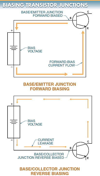
In any transistor circuit, the base/emitter junction must always be forward biased and the base/collector junction must always be reverse biased. See Figure 6.
The external voltage (bias voltage) is connected so that the positive terminal connects to the P-type material (base) and the negative terminal connects to the N-type material (emitter). This arrangement forward biases the base/emitter junction.
Current flows from the emitter to the base. The action that takes place is the same as the action that occurs for a forward-biased semiconductor diode.
In any transistor circuit, the base/collector junction must always be reverse biased. The external voltage is connected so that the negative terminal connects to the P-type material (base) and the positive terminal connects to the N-type material (collector). This arrangement reverse biases the base/collector junction.
Only a very small current (leakage current) flows in the external circuit. The action that takes place is the same as the action that occurs for a semiconductor diode with the reverse bias applied.
Figure 6. In a transistor circuit, the base/emitter junction must always be forward biased and the base/collector junction must always be reverse biased.
Transistor Current Flow
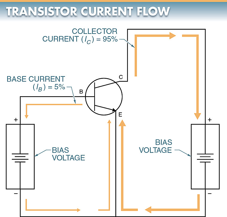
Individual PN junctions can be used in combination with two bias arrangements. The base/emitter junction is forward biased while the base/collector junction is reverse biased. This circuit arrangement results in an entirely different current path than the path that occurs when the individual circuits are biased separately. See Figure 7.
The forward bias of the base/emitter circuit causes the emitter to inject electrons into the depletion region between the emitter and the base.
Because the base is less than 0.001′′ thick for most transistors, the more positive potential of the collector pulls the electrons through the thin base. As a result, the greater percentage (95%) of the available free electrons from the emitter pass directly through the base (IC) into the N-type material, which is the collector of the transistor.
Figure 7. In a transistor, an entirely different current path is created when both junctions are biased simultaneously than when each junction is biased separately.
Transistor Amplifier Key Takeaways
Transistor amplifier plays a crucial role in various applications such as audio amplification, signal processing, and communication systems. By efficiently increasing the amplitude of small signals, they enable devices to function effectively across different industries, from consumer electronics to industrial control systems. Understanding transistor behavior, biasing, and gain characteristics is essential for designing circuits that meet specific performance needs in modern technology.
