The article discusses the use of Zener diode as voltage regulators in DC circuits, explaining their operational behavior in different bias conditions and how they maintain a steady output voltage. It also covers key design considerations such as diode power ratings and load resistance limits to ensure effective voltage regulation.
For many applications, it is desirable that a DC supply be steady and ripple-free. Voltage regulators are used to ensure that the output of a DC supply is steady and relatively independent of load. The most common device employed in voltage regulation schemes is the Zener diode.
Zener diodes are designed and intended to be used when reverse-biased. The basic mechanism behind the Zener reverse breakdown effect was described here. It is important to recall that the mechanisms behind the Zener and avalanche reverse breakdown effects are different. This difference accounts for the difference in the range of breakdown voltages VZ within which each effect dominates. For Zener diodes, VZ is typically no larger than 5.6 V.
A generic diode i-v characteristic, with forward offset voltage V𝛾 and reverse breakdown voltage VZ. Note the steep slope of the i-v characteristic near VZ, which suggests that when vD ≈ −VZ the diode voltage will change very little for large changes in the diode current. It is exactly this property that makes the Zener diode a useful voltage regulator.
Although the slope of the i-v characteristic is not constant near −VZ, for the sake of simplicity in introducing the basic principles of voltage regulation this slope will be assumed to be constant such that a Zener diode can be modeled with linear elements when it is reverse-biased near vD = −VZ.
Like other diodes, a Zener diode has three regions of operation:
- When vD ≥ Vγ, the Zener diode is forward-biased and can be analyzed using the piecewise linear model shown in Figure 1.
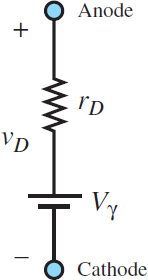
Figure 1 Zener diode model for forward bias
- When −VZ < vD < Vγ, the Zener diode is reverse-biased but has not reached breakdown. In this region, it can be modeled as an open-circuit.
- For vD ≤ –VZ, the Zener diode is reverse-biased and breakdown has ensued. In this region, it can be modeled using the piecewise linear model shown in Figure 2.
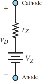
Figure 2 Zener diode model for reverse bias
The combined effect of forward and reverse bias may be lumped into a single model with the aid of ideal diodes, as shown in Figure 3.
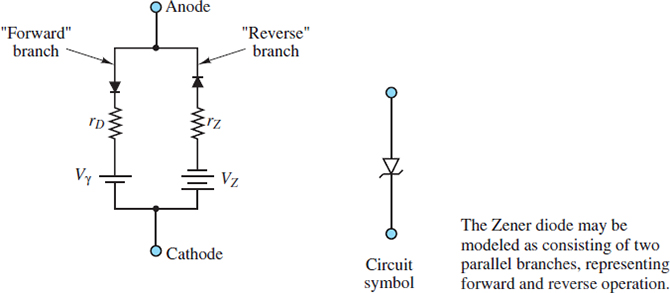
Figure 3 Complete model for Zener diode
To illustrate the operation of a Zener diode as a voltage regulator, consider the circuit of Figure 4(a), where the unregulated DC source VS is regulated to the value of the Zener voltage VZ.
Note how the diode must be connected upside down to obtain a positive regulated voltage. Also note that when vS > VZ the Zener diode is in reverse breakdown. (In practice, it is important that vS remain greater than VZ.)
The source resistance RS is essential because it allows the voltage difference vS −VZ to be non-zero. If the diode resistance rZ is small compared to RS and R, the Zener diode model of Figure 2 can be approximated as a battery of strength VZ, as shown in the simplified circuit of Figure 4(b).
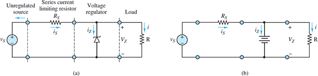
Figure 4 (a) A Zener diode voltage regulator circuit diagram; and (b) the simplest equivalent circuit
Three observations are sufficient to understand the operation of this voltage regulator:
1.The load voltage must equal VZ as long as the Zener diode is in the reverse breakdown mode. Then:
\[i=\frac{{{V}_{Z}}}{R}\begin{matrix}{} & {} & (1) \\\end{matrix}\]
2.The output current is the nearly constant difference between the unregulated supply current iS and the diode current iZ:
\[i={{i}_{S}}-{{i}_{Z}}\begin{matrix}{} & {} & (2) \\\end{matrix}\]
Any current in excess of that required to keep the load at the constant voltage VZ is sent to ground through the diode. Thus, the Zener diode acts as a sink for any undesired source current.
3.The source current is:
\[{{i}_{S}}=\frac{{{v}_{S}}-{{V}_{Z}}}{{{R}_{S}}}\begin{matrix}{} & {} & (3) \\\end{matrix}\]
There are certain considerations that arise in the design of a practical voltage regulator. One of these considerations is the power rating of the diode. The power PZ dissipated by the diode is:
\[{{P}_{Z}}={{i}_{Z}}{{V}_{Z}}\begin{matrix}{} & {} & (4) \\\end{matrix}\]
Since VZ is more or less constant, the power rating establishes an upper limit on the allowable diode current iZ. This limit would be exceeded if the supply voltage rises unexpectedly or if the load is removed such that all the supply current sinks through the diode. The possibility of an open-circuit output must be accommodated in the design of a practical voltage regulator.
Another significant limitation occurs when the load resistance is small, thus requiring large amounts of current from the unregulated supply. In this case, the Zener diode is hardly taxed at all in terms of power dissipation, but the unregulated supply may not be able to provide the current required to sustain the load voltage. In this case, regulation fails to take place. Thus, in practice, the range of load resistances for which load voltage regulation may be attained is constrained to a finite interval:
\[{{R}_{\min }}\le R\le {{R}_{\max }}\begin{matrix}{} & {} & (5) \\\end{matrix}\]
Where Rmax is typically limited by the Zener diode power rating and Rmin by the maximum supply current.
Zener Diode as Voltage Regulator Key Takeaways
Zener diodes play a critical role in voltage regulation due to their ability to maintain a constant output voltage despite variations in load current or supply voltage. This makes them especially valuable in applications requiring stable DC power, such as in power supplies for electronic circuits, communication equipment, and embedded systems. Their simple design, low cost, and reliability contribute to their widespread use in regulating voltage across a specified range of load conditions. By carefully considering parameters like power dissipation and load resistance limits, engineers can design effective and safe voltage regulation circuits that ensure consistent performance, protecting sensitive components from voltage fluctuations.