The article provides an overview of amplifier, focusing on their fundamental roles in electronic systems, ideal characteristics such as high input and low output impedance, and how feedback—especially negative feedback—enhances amplifier performance. It also explains the behavior and gain of ideal and practical amplifier models, highlighting the impact of feedback on stability, linearity, and impedance.
Amplifiers are an essential aspect of many electronic applications. Perhaps the most familiar use of an amplifier is to convert the low-voltage, low-power signal from a digital audio player (e.g., iPhone or MP3 player) to a level suitable for driving a pair of earbuds or headphones, as shown in Figure 1.

Figure 1 Typical digital audio player
Amplifiers have important applications in practically every field of engineering because the vast majority of transducers and sensors used for measurement produce electrical signals, which are then amplified, filtered, sampled, and processed by analog and digital electronic instrumentation. For example, mechanical engineers use thermistors, accelerometers, and strain gauges to convert temperature, acceleration, and strain into electrical signals. These signals must be amplified prior to transmission and then filtered (a function carried out by amplifiers) prior to sampling the data in preparation for producing a digital version of the original analog signal.
Other, less obvious, functions such as impedance isolation are also performed by amplifiers. It should now be clear that amplifiers do more than simply produce an enlarged replica of a signal although that function is certainly very important.
Ideal Amplifier Characteristics
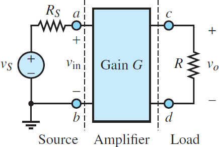
The simplest model for an amplifier is depicted in Figure 2, where a signal vS is amplified by a constant factor G, called the voltage gain of the amplifier. Ideally, the input impedance of the amplifier is infinite such that vin = vS; if its output impedance is zero, vo will be determined by the amplifier independent of R such that:
\[\begin{matrix}{{v}_{0}}=G{{v}_{in}}=G{{v}_{S}} & Ideal\text{ }amplifier & (1) \\\end{matrix}\]

Figure 2 Amplifier between source and load
Note that the input seen by the amplifier is a Thevenin source (vS in series with RS), while the output seen by the amplifier is a single equivalent resistance R.
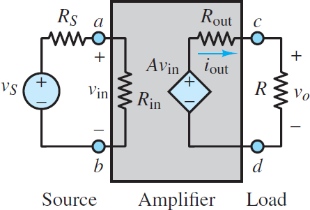
A more realistic (but still quite simple) amplifier model is shown in Figure 3. In this figure the concepts of input and output impedance of the amplifier are incorporated as single resistances Rin and Rout, respectively. That is, from the perspective of the load R the amplifier acts as a Thevenin source (A υin in series with Rout), while from the perspective of the external source (vS in series with RS) the amplifier acts as an equivalent resistance Rin. The constant A is the multiplier associated with the dependent (controlled) voltage source and is known as the open–loop gain.

Figure 3 Simple voltage amplifier model
Using the amplifier model of Figure 3 and applying voltage division, the input voltage to the amplifier is now:
\[{{v}_{ab}}={{v}_{in}}=\frac{{{R}_{in}}}{{{R}_{S}}+{{R}_{in}}}{{v}_{S}}\begin{matrix}{} & {} & (2) \\\end{matrix}\]
The output voltage of the amplifier can also be found by applying voltage division, where:
\[{{v}_{0}}=A{{v}_{in}}\frac{R}{{{R}_{out}}+R}\begin{matrix}{} & {} & (3) \\\end{matrix}\]
Substitute for vin and divide both sides by vS to obtain:
\[\frac{{{v}_{0}}}{{{v}_{S}}}=A\frac{{{R}_{in}}}{{{R}_{S}}+{{R}_{in}}}\frac{R}{{{R}_{out}}+R}\begin{matrix}{} & {} & (4) \\\end{matrix}\]
which is the overall voltage gain from vS to vo. The voltage gain G of the amplifier itself is:
\[G=\frac{{{v}_{0}}}{{{v}_{in}}}=A\frac{R}{{{R}_{out}}+R}\begin{matrix}{} & {} & (5) \\\end{matrix}\]
For this model, the voltage gain G is dependent upon the external resistance R, which means that the amplifier performs differently for different loads. Moreover, the input voltage vin to the amplifier is a modified version of vS. Neither of these results seem desirable. Rather, it stands to reason that the gain of a “quality” amplifier would be independent of its load and would not impact its source signal. These attributes are achieved when Rout ≪ R and Rin ≫ RS. In the limit that Rout → 0:
\[\underset{{{R}_{out}}\to 0}{\mathop{\lim }}\,\frac{R}{{{R}_{out}}+R}=1\begin{matrix}{} & {} & (6) \\\end{matrix}\]
such that:
\[G\equiv \frac{{{v}_{0}}}{{{v}_{in}}}\approx A\begin{matrix}{} & when\begin{matrix}{} & {{R}_{out}}\to 0 \\\end{matrix} \\\end{matrix}\begin{matrix}{} & {} & (7) \\\end{matrix}\]
Also, in the limit that Rin → ∞:
\[\underset{{{R}_{in}}\to \infty }{\mathop{\lim }}\,\frac{{{R}_{in}}}{{{R}_{in}}+{{R}_{S}}}=1\begin{matrix}{} & {} & (8) \\\end{matrix}\]
such that
\[{{v}_{in}}\approx {{v}_{S}}\begin{matrix}{} & when\begin{matrix}{} & {{R}_{in}}\to \infty \\\end{matrix} \\\end{matrix}\begin{matrix}{} & {} & (9) \\\end{matrix}\]
In general, a “quality” voltage amplifier will have a very small output impedance and a very large input impedance.
Input and Output Impedance
In general, the input impedance Rin and the output impedance Rout of an amplifier are defined as:
\[{{R}_{in}}=\frac{{{v}_{in}}}{{{i}_{in}}}\begin{matrix}{} & and\begin{matrix}{} & {{R}_{out}}=\frac{{{v}_{OC}}}{{{i}_{SC}}} \\\end{matrix} \\\end{matrix}\begin{matrix}{} & {} & (10) \\\end{matrix}\]
where vOC is the open-circuit voltage and iSC is the short-circuit current at the output of the amplifier. An ideal voltage amplifier has zero output impedance and infinite input impedance so that the amplifier does not suffer from loading effects at its input or output terminals. In practice, voltage amplifiers are designed to have large input impedance and small output impedance.
It is a worthwhile exercise to show that an ideal current amplifier has zero input impedance and infinite output impedance. Also, an ideal power amplifier is designed so that its input impedance matches its source network and its output impedance matches its load impedance.
Feedback
Feedback, which is the process of using the output of an amplifier to reinforce or inhibit its input, plays a critical role in many amplifier applications.
Without feedback an amplifier is said to be in open–loop mode; with feedback an amplifier is said to be in closed–loop mode. The output of the amplifier model shown in Figure 3 does not affect its input (because there is no path from output to input), so feedback is not present, and the model is open-loop.
As suggested earlier, the most basic characteristic of an amplifier is its gain, which is simply the ratio of the output to the input. The open-loop gain A of a practical amplifier (e.g., an operational amplifier) is usually very large, whereas the closed-loop gain G is a reduced version of the open-loop gain.
There are two types of feedback possible in closed-loop mode: positive feedback, which tends to reinforce the amplifier input, and negative feedback, which tends to inhibit the amplifier input. Both positive and negative feedback have useful applications; however, negative feedback is by far the most common type of feedback found in applications.
In general, negative feedback causes the large open-loop gain A of an amplifier to be exchanged for a smaller closed-loop gain G. While this exchange may seem undesirable at first glance, several key benefits accompany the exchange. These benefits to the amplifier are:
- Decreased sensitivity to variations in circuit and environmental parameters, most notably temperature.
- Increased bandwidth.
- Increased linearity.
- Increased signal-to-noise ratio.
In addition, negative feedback is implemented by establishing one or more paths from the output to the input of the amplifier. The impedance of each feedback path can be adjusted to produce improved input and output impedances of the overall amplifier circuit. These input and output impedances are key characteristics for understanding the loading effects of other circuits attached to an amplifier.
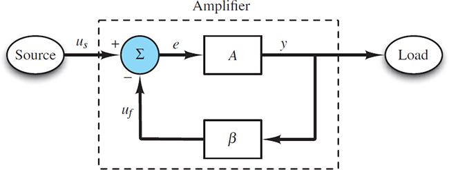
Figure 4 shows a signal–flow diagram of an amplifier situated between a source and a load. The arrows indicate the direction of signal flow. The signals shown are us, uf, e, and y. The output signal of each rectangle is a multiple of its input signal, where the two constants, A and β, are both positive such that:
\[y=Ae\begin{matrix}{} & and\begin{matrix}{} & {{u}_{f}}=\beta y \\\end{matrix} \\\end{matrix}\begin{matrix}{} & {} & (11) \\\end{matrix}\]

Figure 4 Signal-flow diagram of generic amplifier
The circle sums its inputs, us and uf, to produce one output, e. The polarity signs (±) indicate that us and uf make positive and negative contributions to the sum, respectively. That is:
\[e\begin{matrix}={{u}_{s}} & \begin{matrix}- & {{u}_{f}}={{u}_{s}}-\beta y \\\end{matrix} \\\end{matrix}\begin{matrix}{} & {} & (12) \\\end{matrix}\]
Because the feedback signal uf makes a negative contribution to the sum, the signal flow diagram of Figure 4 is said to employ negative feedback.
Equations 11 and 12 can be combined to yield:
\[\begin{matrix}y=Ae= & \begin{matrix}A({{u}_{s}}- & {{u}_{f}})=A({{u}_{s}}-\beta y \\\end{matrix}) \\\end{matrix}\begin{matrix}{} & {} & (13) \\\end{matrix}\]
which can be rearranged to solve for y. Then, the closed-loop gain of the amplifier is:
\[G\equiv \frac{y}{{{u}_{s}}}=\frac{A}{1+A\beta }\begin{matrix}{} & {} & (14) \\\end{matrix}\]
The quantity Aβ is known as the loop gain. Implicit in the derivation of equation 14 is that the behavior of the blocks within the amplifier is not affected by the other blocks nor by the external source and load. In other words, the blocks are ideal such that loading effects are zero.
Two important observations can be made at this point:
- The closed-loop gain G depends upon β, which is known as the feedback factor.
- Since Aβ is positive, the closed-loop gain G is smaller than the open-loop gain A.
Furthermore, for most practical amplifiers, Aβ is quite large such that:
\[G\approx \frac{1}{\beta }\begin{matrix}{} & {} & (15) \\\end{matrix}\]
This result is particularly important (and probably surprising!) because it indicates that the closed-loop gain G of the amplifier is largely independent of the open-loop gain A, as long as Aβ ≫ 1, and that G is, in turn, determined largely by the feedback factor, β.
When Aβ ≫ 1, the closed-loop gain G of an amplifier is determined largely by the feedback factor, β.
Furthermore, equation 14 can be used to find the ratio of the two inputs, us and uf.
\[\frac{{{u}_{f}}}{{{u}_{s}}}=\frac{y}{{{u}_{s}}}\frac{{{u}_{f}}}{y}=\frac{A}{1+A\beta }\beta =\frac{A\beta }{1+A\beta }\begin{matrix}{} & {} & (16) \\\end{matrix}\]
Thus, when Aβ ≫ 1, another important result is:
\[\frac{{{u}_{f}}}{{{u}_{s}}}\to 1\begin{matrix}{} & or\begin{matrix}{} & {{u}_{s}}-{{u}_{f}}\to 0 \\\end{matrix} \\\end{matrix}\begin{matrix}{} & {} & (17) \\\end{matrix}\]
This result indicates that when the loop gain Aβ is large, the difference between the input signal us and the feedback signal uf is driven toward zero.
When Aβ ≫ 1, the difference between the input signal us and the feedback signal uf is driven toward zero.
Both of the results of equations 15 and 17 will show up repeatedly in the analysis of operational amplifier circuits in closed-loop mode.
Benefits of Negative Feedback
Negative feedback provides several benefits in exchange for a reduced gain. For example, take the derivative of both sides of equation 14 to find:
\[dG=\frac{dA}{1+A\beta }-\frac{A\beta dA}{{{(1+A\beta )}^{2}}}=\frac{dA}{{{(1+A\beta )}^{2}}}\begin{matrix}{} & {} & (18) \\\end{matrix}\]
Divide the left side by G and the right side by A/(1 + Aβ) to obtain:
\[\frac{dG}{G}=\frac{1}{1+A\beta }\frac{dA}{A}\begin{matrix}{} & {} & (19) \\\end{matrix}\]
When Aβ ≫ 1, this result indicates that the percentage change in G due to a percentage change in A is relatively small. In other words, the closed-loop gain G is relatively insensitive to changes in the open-loop gain A.
When Aβ ≫ 1, the closed-loop gain G is relatively insensitive to changes in the open-loop gain A.
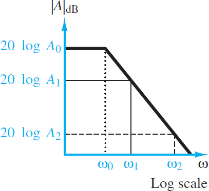
For any amplifier, the open-loop gain A is a function of frequency. For example, the open-loop gain A(ω) of an op-amp is characterized by a simple pole such that:
\[A(\omega )=\frac{{{A}_{0}}}{1+j\omega /{{\omega }_{0}}}\begin{matrix}{} & {} & (20) \\\end{matrix}\]
where ωo is its 3-dB break frequency. The Bode magnitude characteristic plot is shown in Figure 5. Equation 20 can be substituted into equation 14 to obtain:
\[G(\omega )=\frac{A(\omega )}{1+A(\omega )\beta }=\frac{{{A}_{0}}(1+j\omega /{{\omega }_{0}})}{1+{{A}_{0}}\beta (1+j\omega /{{\omega }_{0}})}\begin{matrix}{} & {} & (21) \\\end{matrix}\]

Figure 5 Typical amplifier Bode magnitude characteristic
Multiply the numerator and denominator on the right side of equation 21 by 1 + jω/ωo and then factor out 1 + A0β from the denominator to obtain:
\[G(\omega )=\frac{{{A}_{o}}}{1+{{A}_{o}}\beta }\frac{1}{1+{j\omega }/{{{\omega }_{g}}}\;}={{G}_{0}}\frac{1}{1+j\omega /{{\omega }_{g}}}\begin{matrix}{} & {} & (22) \\\end{matrix}\]
Where ωg = ωo (1 + A0β). Thus, the closed-loop 3-dB break frequency is (1 + A0β) larger than the open-loop 3-dB break frequency.
The closed-loop 3-dB break frequency is (1 + A0β) larger than the open-loop 3-dB break frequency.
Likewise, if the amplifier is characterized by a simple zero, its 3-dB break frequency will be (1 + A0β) smaller than the open-loop 3-dB break frequency. It is a worthwhile exercise to work out this result.
Similar analyses can be performed to show the increased linearity and increased signal-to-noise ratio resulting from negative feedback. All these benefits are acquired at the expense of amplifier gain. Finally, all of the features of a generic amplifier with negative feedback outlined in this section also occur in closed-loop amplifiers constructed using operational amplifiers and other basic components.
Ideal Operational Amplifier Key Takeaways
Understanding amplifiers and their ideal characteristics—such as high input impedance, low output impedance, and proper gain control—is vital for their effective use in a wide range of engineering applications. From enhancing audio signals in consumer electronics to accurately amplifying sensor outputs in industrial measurement systems, amplifiers play a foundational role. The application of feedback, particularly negative feedback, significantly improves amplifier performance by increasing linearity, reducing sensitivity to environmental changes, and refining input/output impedance. These improvements are crucial for building stable, high-performance electronic circuits that interact reliably with various sensors, transducers, and digital systems, making amplifiers indispensable components in modern technology.
