The article provides an overview of the structure and working principle of photovoltaic (PV) cell, focusing on the role of the PN junction in converting sunlight into electricity. It also explains the materials and processes involved in manufacturing PV cells, including the creation of silicon wafers and the formation of electron-hole pairs through solar energy.
The key feature of conventional Photovoltaic PV (solar) cells is the PN junction. In the PN junction solar cell, sunlight provides sufficient energy to the free electrons in the n region to allow them to cross the depletion region and combine with holes in the p region. This energy creates a potential difference (voltage) across the cell.
When an external load is connected, the electrons flow through the semiconductor material and provide current to the external load.
Photovoltaic (PV) Cell Structure
Although there are other types of solar cells and continuing research promises new developments in the future, the crystalline silicon PV cell is by far the most widely used.
A silicon photovoltaic (PV) cell converts the energy of sunlight directly into electricity—a process called the photovoltaic effect—by using a thin layer or wafer of silicon that has been doped to create a PN junction.
The depth and distribution of impurity atoms can be controlled very precisely during the doping process. As shown in Figure 1, the thin silicon circular wafers are first sliced from an ingot of ultra-pure silicon and then the surface of the wafer is textured for better light absorption.
The circular wafer may be trimmed to an octagonal, hexagonal, or rectangular shape for maximum coverage when fitted in a module.
One commonly used process for creating an ingot is called the Czochralski method. In this process, a seed crystal of silicon is dipped into melted silicon. As the seed crystal is withdrawn and rotated, a cylindrical ingot of silicon is formed.

Figure 1: Making a Wafer from a Silicon Ingot
The silicon wafer is doped to create the PN junction structure. The n region is much thinner than the p region to permit light penetration. As shown in Figure 2(a), a grid of very thin conductive contact strips is deposited on top of the wafer by methods such as photoresist or silkscreen.
The contact grid must maximize the surface area of the silicon wafer that will be exposed to the sun in order to collect as much light energy as possible.
The conductive grid is necessary so that the electrons have a shorter distance to travel through the silicon when an external load is connected.
The more distance an electron travels through a material, the more the energy loss due to the inherent resistance of the material. A solid contact covering the bottom of the wafer is then added, as indicated in Figure 2(a).
After the contacts are incorporated, an anti-reflective coating is placed on top of the contact grid and n region.
The purpose of the coating is to allow the PV cell to absorb as much of the sun’s energy as possible by reducing the amount of light energy reflected away from the surface of the cell.
The thickness of the PV cell compared to the surface area is greatly exaggerated for purposes of illustration. In some PV cells, the contact grid is embedded in a textured surface consisting of tiny pyramid shapes that result in improved light capture.
A small segment of a cell surface is illustrated in Figure 2(b). A complete PV cell with a standard surface grid is shown in Figure 3.
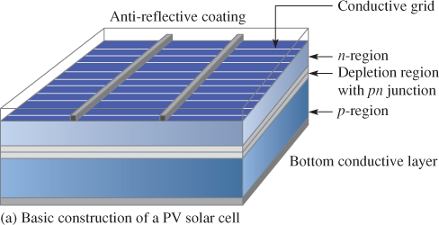
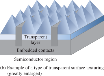
Figure 2: Basic Construction of a Photovoltaic (PV) Solar Cell and an Example of Transparent Surface Texturing
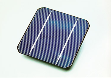
Figure 3: Complete Photovoltaic PV Solar Cell
Photovoltaic (PV) Cell Working Principle
Sunlight is composed of photons or packets of energy. The sun produces an astonishing amount of energy. The small fraction of the sun’s total energy that reaches the earth is enough to meet all of our power needs many times over if it could be harnessed. Sufficient solar energy strikes the earth each hour to meet worldwide demands for an entire year.
The n-type layer of a PV cell is very thin to allow light penetration into the p-type region. The thickness of the entire cell is actually about the thickness of an eggshell.
When a photon penetrates either the n region or the p region and strikes a silicon atom near the PN junction with sufficient energy to knock an electron out of the valence band, the electron becomes a free electron and leaves a hole in the valence band. This is called an electron-hole pair.
The amount of energy required to free an electron from the valence band of a silicon atom is called the band gap and is 1.12 eV (electron volts). The electron volt is a unit of energy used for convenience at the atomic level and specifically for electrons.
In the p region, the free electron is swept across the depletion region by the electric field into the n region. Electrons accumulate in the n region, creating a negative charge.
In the n region, the hole is swept across the depletion region by the electric field into the p region. The electrons that accumulate in the n region create a negative charge, and holes that accumulate in the p region, create a positive charge. A voltage is developed between the n region and p region contacts.
When a load is connected to a PV cell, the free electrons flow out of the n region to the grid contacts on the top surface, out the negative contact, through the load, back into the positive contact on the bottom surface, and then into the p region, where they can recombine with holes.
The sunlight energy continues to create new electron-hole pairs and the process goes on, as illustrated in Figure 4.
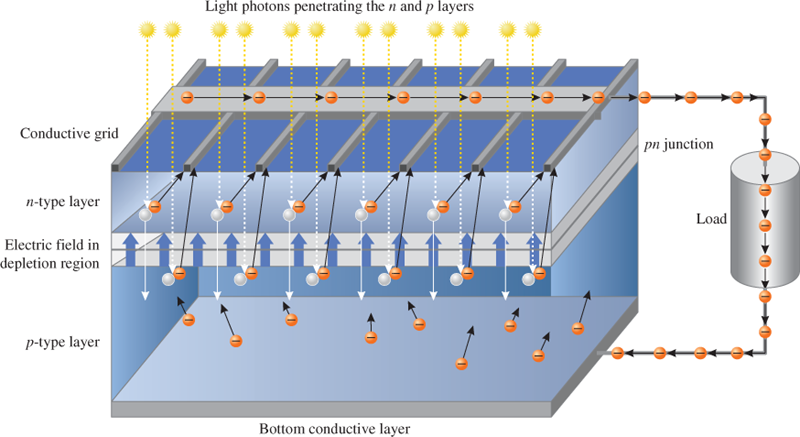
Figure 4: Working of a Photovoltaic (PV) Cell with Incident Sunlight
Review Questions
- Name the parts of a crystalline silicon PV cell.
- Why is the contact on the top surface in the form of a grid?
- What happens if a photon with sufficient energy penetrates into the p region?
- What is band-gap energy?
- What is an electron-hole pair?
Answers
- In addition to the n and p regions and the boundary region, there is an anti-reflective coating and conductive grid on the top and a conductive layer on the bottom.
- The grid allows light to penetrate into the cell.
- An electron-hole pair is created and a voltage develops across the junction.
- Band-gap energy is the energy required to free an electron from the valence band.
- An electron-hole pair is a result when an electron is freed from a crystalline substance and leaves behind a vacancy in the lattice structure.
Photovoltaic (PV) Cell Key Takeaways
Understanding the structure and working principle of photovoltaic (PV) cells—particularly the crucial role of the PN junction—is essential for appreciating their real-world applications. PV cells lie at the heart of solar panels, which are increasingly used in residential, commercial, and industrial energy systems due to their ability to convert sunlight directly into electricity with no moving parts or emissions. The detailed design elements, such as doping processes, surface texturing, and anti-reflective coatings, significantly enhance the efficiency and reliability of solar energy systems. These innovations not only improve performance but also reduce manufacturing costs, making solar power more accessible and sustainable.