This guide covers the JFET working principle, Characteristics Curves, Circuit Configurations (N-Channel and P-Channel), and Applications along with circuit diagrams.
A junction field-effect transistor (JFET) is a simple FET with a PN junction in which output current is controlled by an input voltage. The two types of JFETs include the N-channel and P-channel.
A JFET, like all FETs, contains a gate (G), drain (D), and source (S). The gate is a control element, while the drain and source provide the same function as the emitter and collector on a bipolar junction transistor. See Figure 1.
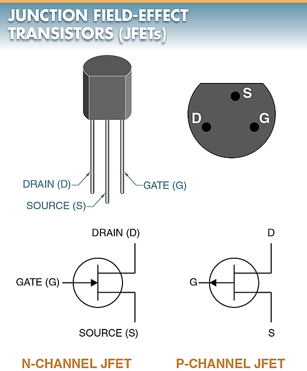
Figure 1. The arrow in a schematic symbol for an N- channel JFET points inward. The arrow points outward for a P-channel JFET.
JFETs may be used as switches and gates. JFETs are even found in voltage regulators and current limiters. JFETs are fully compatible with other semiconductor devices, such as standard bipolar transistors, silicon- controlled rectifiers, triacs, and ICs.
JFET Operation
A JFET is a unipolar device, which differs in operation from a bipolar junction transistor. The output current of a JFET is controlled by the voltage on the gate. The gate voltage creates an electrical field, or depletion region, within the device. See Figure 2.
The JFET is considered a voltage-driven device rather than a current-driven device like the bipolar junction transistor.
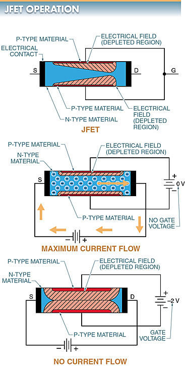
Figure 2. The output current of a JFET is controlled by an electrical field created by the input voltage.
The source and drain of the JFET are connected to a common N-type material. This common material constitutes the channel of the JFET.
If a DC potential is connected between the source and the drain, the current should flow in the external circuit and through the channel.
At zero gate voltage, channel height is maximum and channel resistance is minimum, resulting in current flow. With a slightly positive voltage, the channel height opens further, allowing maximum current flow.
The two sections of P-type material constitute the gate. Each section has its associated electrical field (depletion region).
If the gate is made negative with respect to the channel, the diodes (formed by the P-type and N-type materials) become reverse biased and the depletion regions increase.
At a large enough gate-to-source voltage (VGS), the channel is effectively “pinched off” because of the depletion regions touch. The depletion regions merge at a particular VGS of somewhere between 1 V and 8 V.
The size of the depletion region is controlled by the gate-to-source voltage (VGS). When VGS increases, the depletion region increases. When VGS decreases, the depletion region decreases.
This gate-to-source voltage (VGS) controls the drain current and must always provide a reverse-bias voltage. This is quite different from a bipolar transistor.
In a bipolar transistor, the junction must be forward biased so that the junction impedance is extremely low and there is current flow in the junction.
In a JFET, the junction must be reverse biased so that the junction impedance is high and there is little current flow in the junction. The major advantage of this is good control using voltage rather than current.
The power consumption of the JFET (in standby operation) is thousands of times less than that of a bipolar transistor controlling the same function.
JFET Output Characteristic Curves
A JFET characteristic curve shows the operating characteristics of a JFET. See Figure 3. The drain-source voltage (VDS) is plotted along the horizontal axis. The drain current (ID) is plotted along the vertical axis on the characteristic curve for a typical N-channel JFET.
By using one curve, the detailed information produced may be more readily obtained.
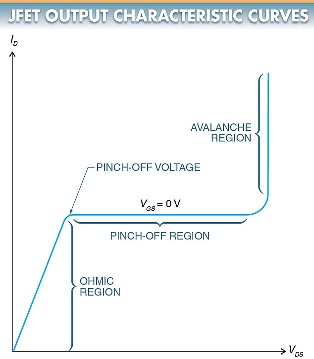
Figure 3. A JFET characteristic curve shows the operating characteristics of a JFET.
Ohmic Region
The ohmic region is the first portion of the characteristic curve of a JFET where the drain current rises rapidly. In the ohmic region, the drain current is controlled by the drain-source voltage and the resistance of the channel.
Pinch-Off Region
The knee of the curve is the pinch-off voltage. On the flattened portion of the graph, the JFET is at the pinch-off region. In this region, the drain current is controlled primarily by the width of the channel.
Avalanche (Breakdown) Region
When the drain current begins another sharp increase, avalanche (breakdown) begins. At this point, a large amount of current begins to pass through the channel. If this current is not limited by an external resistance or load, the JFET may be damaged.
Junction Field-Effect Transistor Circuit Configuration
JFETs can be connected into three basic circuit configurations: common source, common gate, and common drain.
Common-gate and common-drain circuits are constructed in a similar common element arrangement. Furthermore, the only difference between an N-channel and P-channel circuit configuration is the direction of electron flow in the external circuit and the polarity of the bias voltages. See Figure 4.
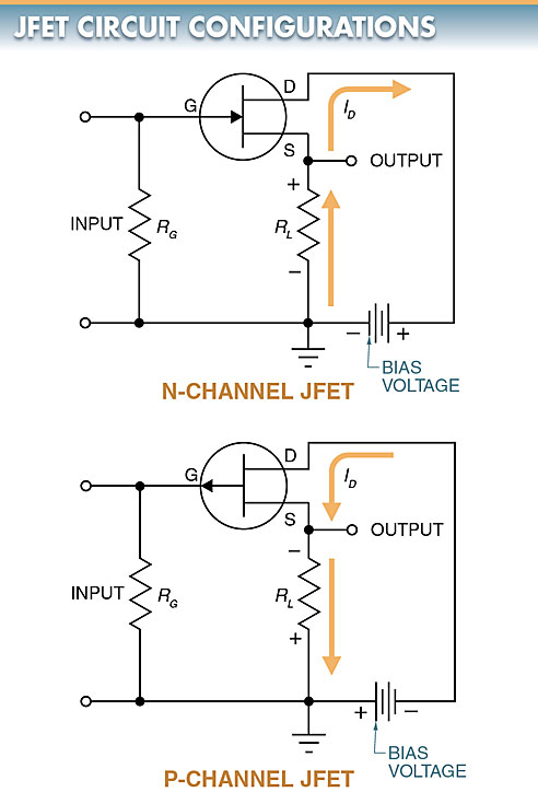
Figure 4. In a common-source JFET circuit, the input is across the gate and source terminals and the output is across the drain and source terminals.
Junction Field-Effect Transistor Applications
JFETs are used extensively in circuits where low power and high impedance are factors. JFETs need very little power to produce a large output at the load.
JFETs are used in many amplifier configurations because they can amplify a fairly wide range of frequencies and have high input impedance. High input impedance is a definite advantage in the transfer of power.
FET multimeters use JFETs to provide high input impedances with good sensitivity. A JFET is capable of producing an input of 11 MΩ or more.
In a simple FET multimeter circuit, the JFET is one “leg” in the DC Bridge. Source resistor RS provides negative feedback for high linearity in the response. The circuit requires good regulation, which is provided by a Zener diode. See Figure 5.
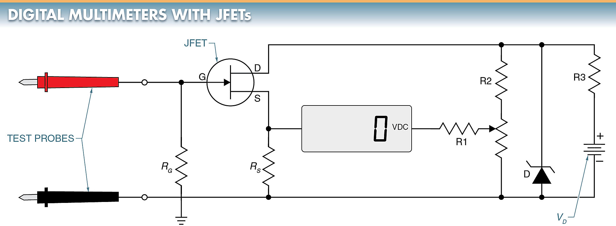
Figure 5. A digital multimeter can provide high input impedance with good sensitivity by using a JFET in its front-end circuit.
Junction Field-Effect Transistor (JFET) Key Takeaways
Understanding the working principle, characteristics, and circuit configurations of JFETs is essential for applying them effectively in modern electronic systems. Due to their high input impedance, low power consumption, and voltage-controlled operation, JFETs are highly valuable in applications such as amplifiers, switches, voltage regulators, and digital multimeters. Their ability to provide stable, linear, and efficient performance makes them especially useful in sensitive analog circuits and instrumentation where signal integrity is crucial.