A metal-oxide semiconductor field-effect transistor (MOSFET) is a three-terminal or four-terminal electronic switching device with metal-oxide or polysilicon insulating material that can be used for amplification. MOSFETs have the same terminal designations (gate, drain, and source) as JFETs.
The gate voltage of a MOSFET that controls the drain current is different from that of a JFET. The main difference in operation between a JFET and MOSFET is that voltage is applied between the gate and the P and N regions of the MOSFET structure. An electric field is generated, penetrates through the oxide layer, and creates an inversion layer, or channel, at the semiconductor-insulator layers.
Varying the voltage between the gate and the P and N layers controls the conductivity of this layer, allowing current to flow between the drain and source.
MOSFETs can operate in either an enhancement mode or a depletion mode.
MOSFET Schematic Symbols and Lead Identification
MOSFETs are available as N-channel and P-channel devices. With an N-channel MOSFET, the arrow on the substrate points toward the channel. With a P-channel MOSFET, the arrow on the substrate points away from the channel. See Figure 6.
Enhancement MOSFET Working
The main body of an enhancement MOSFET is composed of a highly resistive P-type material. Two low-resistance N-type regions are diffused in the P-type region, forming the source and drain.
When the source and drain are completely diffused, the surface of the MOSFET is covered with a layer of insulating material. The insulating layer of the MOSFET is silicon dioxide (SiO2).
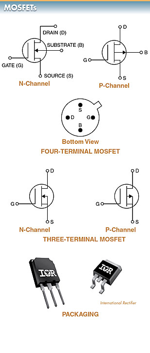
Figure 6. MOSFETs are available in both N-channel and P-channel constructions.
Holes are cut into the silicon dioxide insulating material, allowing contact with the N-type regions and thereby connecting the source and drain leads.
The MOSFET construction is complete when a polysilicon contact (gate) is placed over the insulating material in a position to cover the channel from source to drain. See Figure 7.
Applying the principle of capacitance to the enhancement MOSFET, the gate can be used to produce a conductive channel from the source to the drain. The positive charge of a positive voltage placed on the gate induces a negative charge on the P-type material.
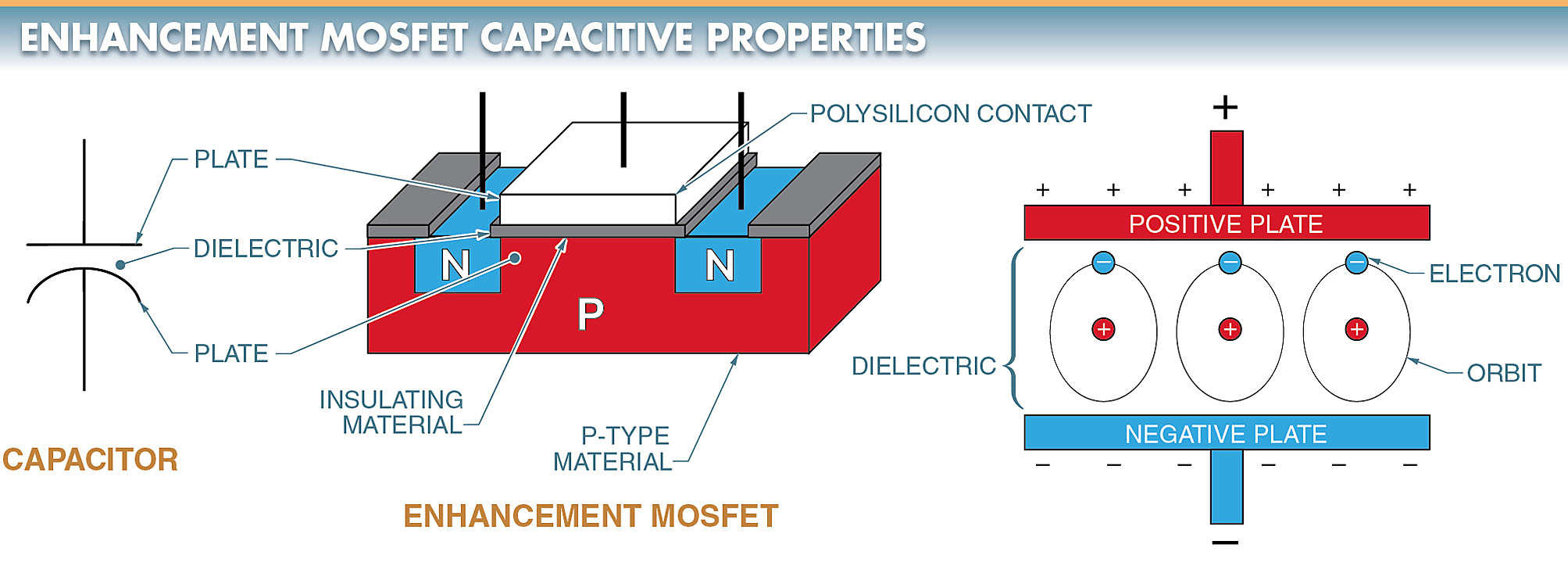
Figure 7. A positive voltage applied to the upper plate of a capacitor causes the dielectric to become distorted, with the electrons moving in the direction of the positive plate.
With increasing positive voltage, the holes in the P-type material are repelled until the region between the source and drain becomes an N-channel. Once the N-channel is forward biased between the source and gate, current begins to flow.
Since electrons have been added to form the N- channel, this MOSFET has enhanced current flow resulting from the application of a positive gate voltage. With a more positive gate voltage, the channel becomes wider. Therefore, current flows from source to drain due to the decreased channel resistance.
When the gate has zero voltage or a negative voltage, no enhancement effect is possible and the MOSFET does not conduct. Since the enhancement MOSFET does not conduct at zero gate voltage, it is often called a normally-off MOSFET.
In the schematic symbol, a broken line between terminals indicates the channel. The broken line signifies that the MOSFET is normally off. See Figure 8.
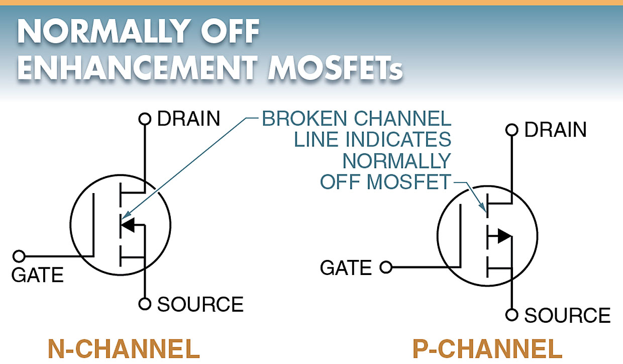
Figure 8. The broken line in the schematic symbol indicates that the MOSFET is normally off.
Depletion-Enhancement MOSFET Working
A depletion-enhancement MOSFET is constructed similarly to the enhancement MOSFET. The main difference is the addition of a physical conducting channel between the source and drain. The presence of the channel allows current to flow from source to drain, even without a gate voltage. See Figure 9.
The depletion-enhancement MOSFET has the same capacitive effect as the enhancement MOSFET. However, when a negative voltage is applied to the gate, holes from the P-type material are attracted into the N-channel. The holes neutralize the free electrons. The result is that the N-channel is depleted, or reduced, in the number of carriers.
The depletion of carriers increases channel resistance and reduces the current. Depletion mode is the operation of a MOSFET with a negative gate voltage.
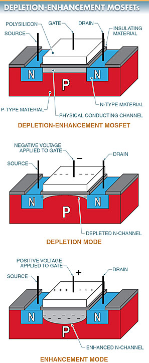
Figure 9. A depletion-enhancement MOSFET has the addition of a physical conducting channel between the source and the drain. In the depletion mode, a negative voltage is applied to the gate; in the enhancement mode, a positive voltage is applied to the gate.
With a positive gate voltage, the N-channel MOSFET can operate in the enhancement mode. Enhancement mode is the operation of a MOSFET with a positive gate voltage. The positive gate voltage widens the N-channel, causing an increase in channel current.
Since the depletion-enhancement MOSFET conducts a significant current even when VGS is zero, it is often called a normally on MOSFET.
Dual-Gate MOSFET Operation
A MOSFET can be constructed with two gates such as in a dual-gate MOSFET arrangement. Current through the MOSFET can be cut off by either gate. A MOSFET also operates on the capacitive effect. See Figure 10.
The dual-gate arrangement allows the MOSFET to be used in a variety of circuits. For example, in a gain control circuit, the audio signal is applied to Gate 1 and the gain control voltage is applied to Gate 2. The gain control voltage can then be used to control the output from Gate 2.
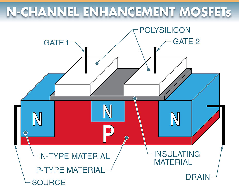
Figure 10. Current through a dual-gate MOSFET can be cut off by either gate.
Power MOSFET Working
Power MOSFETs exhibit the properties of small-signal MOSFETs but are designed to handle higher currents. Power MOSFETs were designed primarily for switching applications.
Power MOSFETs can switch faster than bipolar transistors. Unlike the small-signal MOSFET, the power MOSFET is fabricated with a vertical rather than lateral structure.
MOSFETs are made using the double diffused metal-oxide substrate (DMOS) process and use polysilicon gates. The gate of this device is isolated from the source by a layer of insulating silicon dioxide. When a voltage is applied between the gate and source terminals, an electric field is set up within the MOSFET. This field alters the resistance between the drain and source terminals.
The DMOS power MOSFET contains an inherent PN-junction diode. Its equivalent circuit can be considered as a diode in parallel with the source-to-drain channel, as shown in the schematic symbol. See Figure 11.
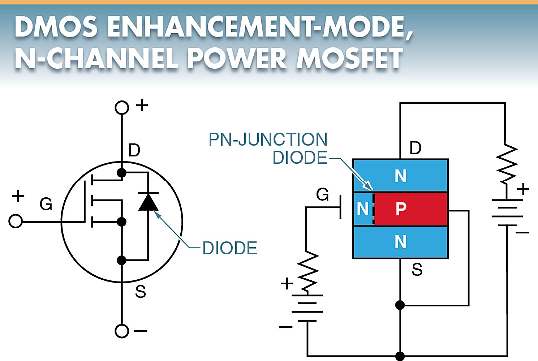
Figure 11. The DMOS power MOSFET contains an inherent PN-junction diode (its equivalent circuit can be considered as a diode in parallel with the source-to-drain channel).
Power MOSFETs as Switches
There are a variety of solid-state switch technologies available to perform switching functions. Each switch technology, however, has strong and weak points.
The ideal switch would have zero resistance in the ON state, infinite resistance in the OFF state, switch instantaneously and would require minimum input power to make it switch.
The primary characteristics that are most desirable in a solid-state switch are fast switching speed, simple drive requirements, and low conduction loss.
For low voltage applications, power MOSFETs offer extremely low ON resistance and approach characteristics of the desired ideal switch.
Power MOSFETs have a wide range of specifications for high-frequency switching power supplies at frequencies above 100 kHz. The advantages of using power MOSFETs overpower bipolar transistors include the following:
- faster switching
- lower switching losses
- wider safe operating area (SOA)
- simple drive circuitry
- ability to be paralleled easily (the forward voltage drops increases with increasing temperature, ensuring an even distribution of current among all components)
