The article provides an overview of enhancement-mode MOSFET, focusing on their structure, operation principles, and behavior under various gate and drain voltages. It also explains the different operating regions—cutoff, ohmic, triode, and saturation—and how current conduction is influenced by gate voltage and device parameters.
Figure 1 depicts the circuit symbol and the construction of a typical n-channel enhancement-mode MOSFET. The device has four regions: the gate, the drain, the source, and the bulk. Each of these regions has its own conducting terminal. The bulk and source terminals are often electrically connected, in which case the bulk terminal is not shown in the circuit symbol. The gate consists of a conducting plate separated from the p-type bulk by a thin (10−9 m) insulating layer, usually silicon oxide SiO2. The drain and source regions are both composed of n+ material.
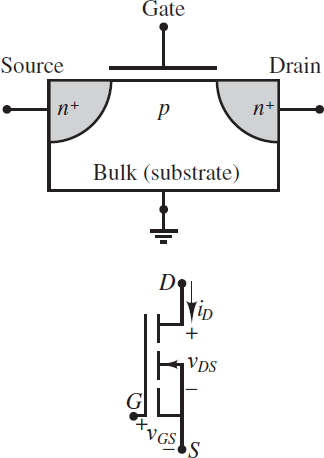
Figure 1 The n-channel enhancement MOSFET construction and circuit symbol
Consider the case when the gate and source terminals are connected to a reference node and the drain terminal is connected to a positive voltage supply VDD, as shown in Figure 2(a). The bulk terminal is also connected to the reference node, by virtue of its connection to the source terminal, and so the pn+ junction between the bulk and drain is reverse-biased.
Likewise, the voltage across the pn+ junction between the bulk and the source is zero, and thus that junction is also reverse-biased. Thus, a path between drain and source consists of two reverse-biased pn+ junctions such that the current from drain to source is effectively zero. In this case, the resistance from drain to source is on the order of 1012 Ω.
When the voltage from gate to source is zero, the n-channel enhancement-mode MOSFET acts as an open-circuit. Thus, enhancement-mode devices are referred to as normally off and their channels as normally open.
Suppose now that a positive DC voltage VGG is applied to the gate as shown in Figure 2(b). Positive majority charge carriers in the bulk (i.e., holes) are repelled in the region nearest the gate. At the same time, negative majority charge carriers in the source and drain (i.e., electrons) are drawn to the same region. The result is a narrow n-type channel beneath the insulating layer that separates the gate from the bulk. For a given drain voltage, the higher the gate voltage, the higher the concentration of negative charge carriers in the channel, and the higher its conductivity.
The term enhancement mode refers to the influence of the gate voltage in enhancing the conductivity of the channel. The term field effect refers to the effect of the electric field from gate to bulk that is associated with the gate voltage.
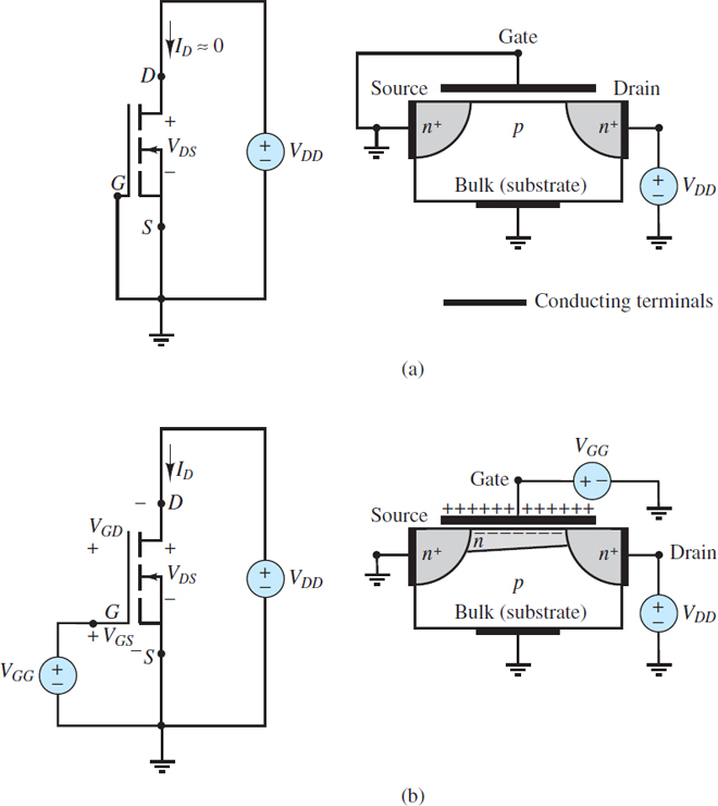
Figure 2 Channel formation in NMOS transistor: (a) With zero gate voltage, the source-bulk and bulk-drain junctions are both reverse-biased, and the channel acts as an open-circuit; (b) when a positive gate voltage is applied, positive majority carriers in the bulk (i.e., holes) are repelled by the gate leaving behind negatively charged atoms. Also, negative majority carriers from the source and drain (i.e., electrons) are drawn toward the gate. The result is a conducting n-type channel between the source and drain regions.
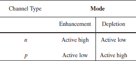
Depletion-mode devices also exist, in which an externally applied field depletes the channel of charge carriers by reducing the effective channel width. Depletion-mode MOSFETs are normally on (i.e., the channel is conducting) and are turned off (i.e., the channel is not conducting) by an external gate voltage.
Both enhancement- and depletion-mode MOSFETs are available with either n– or p-type channels. Enhancement-mode devices do not have a conducting channel built in; however, one can be created by the action of the gate.
On the other hand, depletion-mode devices do have a built-in conducting channel that can be depleted by the action of the gate. Depending upon the mode and channel type, FETs can be active high or active low devices, where high and low refer to the voltage of the gate relative to a common reference.
Table 1 summarizes these results. n– and p-channel MOSFETs are referred to as NMOS and PMOS transistors, respectively.
Table 1
Operating Regions and the Threshold Voltage Vt
When the gate-to-bulk voltage of an NMOS transistor (See Figure 3) is less than a threshold voltage Vt, a channel will not form between the source and drain. The result is that no current can be conducted from drain to source and the transistor is in the cutoff region. Typical values of Vt are between 0.3 and 1.0 V, although it can be significantly larger.
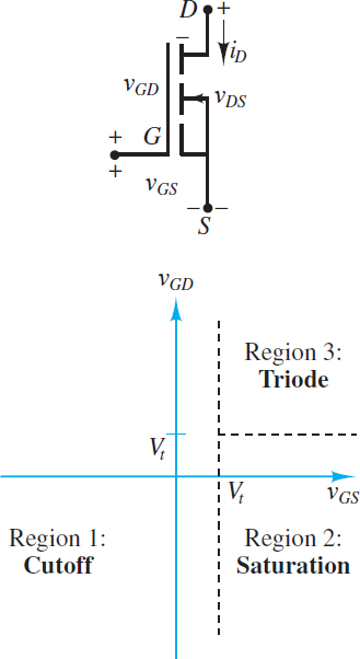
Figure 3 Regions of operation of NMOS transistor
When the gate-to-bulk voltage is greater than the threshold voltage Vt at any point between the source and drain, a conducting n-type channel is formed at that point. If, as usual, the source and bulk are both connected to a common reference, then the gate-to-bulk voltage is the same as the gate-to-source voltage vGS.
If the drain is also connected to the same common reference such that vDS = 0, then a channel of uniform thickness will be formed from drain to source when vGS > Vt. It is common to introduce the overdrive voltage vOV = vGS − Vt, which is the gate-to-source voltage in excess of what is necessary to create a channel. Note that vOV > 0 is another way to write vGS > Vt.
Note that if vDS = 0, then ${{v}_{GD}}\equiv {{v}_{GS}}-{{v}_{DS}}={{v}_{GS}}$, the channel has a uniform thickness, and its resistance per unit channel length is also uniform. In this state, known as the ohmic region, the channel effectively acts as a variable resistor whose resistance is dictated by the gate voltage.
In other words, for a given value of vGS, the channel current iD is proportional to vDS. This linear relationship between iD and vDS is valid for small values of vDS.
\[\begin{matrix}{{i}_{D}}\propto {{v}_{DS}} & when & \begin{matrix}{{v}_{DS}}\ll {{v}_{OV}} & \text{Ohmic Region} & (1) \\\end{matrix} \\\end{matrix}\]
When vGS > Vt and the drain-to-source voltage vDS is no longer small but held at a positive value VDD, the channel is thinner near the drain than near the source, as depicted in Figure 2(b).
In addition, as long as vGD > Vt, the channel will still exist from source to drain. This condition is equivalent to the requirement that vDS < vOV. In this state, the channel resistance per unit length is no longer uniform, the channel current iD is proportional to$v_{DS}^{2}$, and the transistor is in the triode region.
\[\begin{matrix}\begin{matrix}{{i}_{D}}\propto {{v}^{2}}_{DS} & when & {{v}_{DS}}<{{v}_{OV}} \\\end{matrix} & \text{Triode Region} & \left( 2 \right) \\\end{matrix}\]
It is important to realize that the ohmic region is simply one part of the triode region when vDS « vOV.
Eventually, if vDS is continually increased, it will exceed vOV such that the channel thickness at the drain goes to zero. In fact, the depletion region of the bulk-drain junction has expanded sufficiently, due to the increase in vDS, to take the place of the channel. This condition is often called channel pinch-off. Although the channel thickness is now zero, current is still conducted in the channel because the voltage at the drain is large enough to drive mobile electrons in the channel across the depletion region.
However, any increase in vDS beyond vOV is confined to the depletion region such that the voltage across the channel length remains constant. The result is that the channel current is independent of vDS and depends only upon vOV. In this state, the transistor is in the saturation region.
\[\begin{matrix}\begin{matrix}{{i}_{D}}\propto {{v}^{2}}_{OS} & when & {{v}_{DS}}>{{v}_{OV}} \\\end{matrix} & \text{Saturation Region} & (3) \\\end{matrix}\]
These operating regions and their dependence upon vGD and vGS are depicted in Figure 3.
Channel Current iD and the Conductance Parameter K
The ability of the channel to conduct is dependent on various mechanisms, the effects of which are captured in a conductance parameter K, defined as:
\[K=\frac{W}{L}\frac{\mu {{C}_{ox}}}{2}\begin{matrix}{} & {} & (4) \\\end{matrix}\]
Where W is the cross-sectional width of the channel, L is the channel length, μ is the mobility of the majority channel charge carrier (electrons in n-channel devices, holes in p-channel devices), and Cox is the gate-channel capacitance due to the thin insulating oxide layer. The units of K are A/V2.
With this definition of the conductance parameter, the relationship between iD and vDS can be expressed in the various operating regions as listed here. In the cutoff region:
\[\begin{matrix}\begin{matrix}{{i}_{D}}=0 & when & {{v}_{GS}}\ll V \\\end{matrix} & \text{Cutoff Region} & (5) \\\end{matrix}\]
In the triode region:
\[\begin{matrix}\begin{matrix}{{i}_{D}}=K(2{{v}_{OV}}-{{v}_{DS}}){{v}_{DS}} & when & {{v}_{DS}}<{{v}_{OV}} \\\end{matrix} & \text{Triode Region} & (6) \\\end{matrix}\]
When vDS << vOV, this expression is approximated by
\[\begin{matrix}\begin{matrix}{{i}_{D}}\approx 2K{{v}_{OV}}{{v}_{DS}} & when & {{v}_{DS}}\ll {{v}_{OV}} \\\end{matrix} & \text{Ohmic Region} & (7) \\\end{matrix}\]
Which is the linear relationship characteristic of the ohmic region. In the ohmic region, the transistor acts as a voltage-controlled resistor. This property allows transistors to act as resistors in integrated circuit (IC) designs. Other applications of a voltage-controlled resistor are found in tunable (variable-gain) amplifiers and in analog gates.
In the saturation region:
\[\begin{matrix}\begin{matrix}{{i}_{D}}\approx Kv_{OV}^{2} & when & {{v}_{DS}}>{{v}_{OV}} \\\end{matrix} & \text{Saturation Region} & (8) \\\end{matrix}\]
This relationship is only approximate. This relationship is made more exact by accounting for the Early effect, which describes the effect of vDS on the effective length of the channel. This effect is accounted for by incorporating the Early voltage VA as:
\[\begin{matrix}\begin{matrix}{{i}_{D}}=Kv_{OV}^{2}\left( 1+\frac{{{v}_{DS}}}{{{V}_{A}}} \right) & when & {{v}_{DS}}>{{v}_{OV}} \\\end{matrix} & \text{Saturation Region} & (9) \\\end{matrix}\]
When VA is large compared to vDS, as is often the case, the Early effect is small and equation 9 is well approximated by equation 8. When this condition is true, the transistor acts as a voltage-controlled current source.
The three regions of operation can also be identified in the characteristic curves shown in Figure 4, which can be generated from the circuit of Figure 2(b) by varying the gate and drain voltages relative to the source voltage.
Notice that for vGS < Vt the transistor is in the cutoff region and iD = 0. The boundary between the saturation and triode regions is indicated by the curve${{i}_{D}}=Kv_{DS}^{2}$, which is the locus of all points where the slope of the characteristic curve first becomes zero as vDS increases. (If the Early voltage VA is not negligible, then the slope of the characteristic lines in saturation is not zero, but some small positive constant.)
In the saturation region, the transistor drain current is nearly constant and independent of vDS. In fact, its value is proportional to $v_{GS}^{2}$.
Finally, in the triode region, the drain current is strongly dependent on vGS and vDS. As vDS → 0 the slope of each characteristic curve becomes approximately constant, which is the characteristic of the ohmic region.
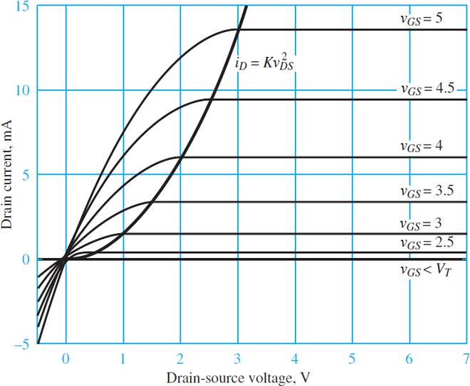
Figure 4 Characteristic drain curves for an NMOS transistor with Vt = 2 V and K = 1.5 mA/V2
Operation of the P-channel Enhancement-Mode MOSFET
The operation of a PMOS enhancement-mode transistor is very similar in concept to that of an NMOS device. Figure 5 depicts a test circuit and a sketch of the device construction.
Note that the roles of the n-type and p-type materials are reversed and that the charge carriers in the channel are holes, not electrons. Further, the threshold voltage Vt is now negative. However, if vGS is replaced with vSG, vGD with vDG, and vDS with vSD, and |Vt| is used in place of Vt, then the analysis of the device is completely analogous to that of an NMOS transistor.
In particular, Figure 6 depicts the behavior of a PMOS transistor in terms of the gate-to-drain and gate-to-source voltages, in analogy with Figure 3. The resulting equations for the three modes of operation of the PMOS transistor are summarized below:
Cutoff region: when vSG < |Vt | and vDG < |Vt |.
\[{{i}_{D}}=0\begin{matrix}{} & Cutoff\text{ }region & (10) \\\end{matrix}\]
Saturation region: when vSG > |Vt | and vDG < |Vt |.
\[{{i}_{D}}\cong K{{\left( {{v}_{SG}}-\left| {{V}_{t}} \right| \right)}^{2}}\begin{matrix}{} & Saturation\text{ }region & (11) \\\end{matrix}\]
Triode region: when vSG >|Vt| and vDG >|Vt|.
\[{{i}_{D}}=K\left[ 2{{\left( {{v}_{SG}}-\left| {{V}_{t}} \right| \right)}^{2}}{{v}_{SD}}-v_{SD}^{2} \right]\begin{matrix}{} & Triode\text{ }or\text{ }ohmic\text{ }region & (12) \\\end{matrix}\]
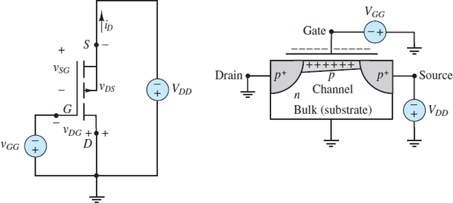
Figure 5 The p-channel enhancement-mode field-effect transistor (PMOS)
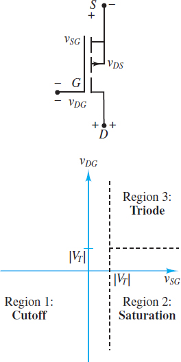
Figure 6 Regions of operation of PMOS transistor
Enhancement Mode MOSFET Key Takeaways
Understanding the structure, operation, and various regions of enhancement-mode MOSFET is crucial for their effective use in electronic circuits. These devices play a fundamental role in modern digital and analog electronics due to their high input impedance, scalability, and fast switching characteristics. Their ability to operate in distinct regions—cutoff, ohmic, triode, and saturation—makes them highly versatile for applications such as signal amplification, digital logic gates, and voltage-controlled resistors. In integrated circuits, especially CMOS technology, enhancement-mode MOSFET are essential building blocks.