The article provides an overview of Insulated Gate Bipolar Transistor (IGBT) operation, characteristics, and configurations, highlighting its structure, switching behavior, and safe operating conditions. It also compares IGBT types (PT and NPT) and discusses factors affecting performance and protection in high-power applications.
An insulated gate bipolar transistor (IGBT) is a three-terminal switching device that combines an FET for control with a bipolar transistor for switching. See Figure 1.
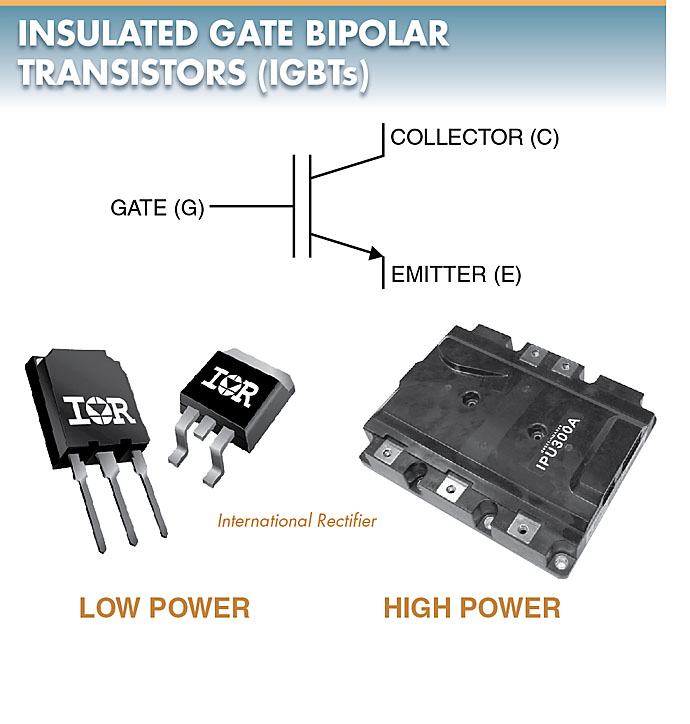
Figure 1. An insulated-gate bipolar transistor (IGBT) is a three-terminal switching device that combines a FET with a bipolar transistor.
Insulated Gate Bipolar Transistor Characteristics
The main difference in construction between the power MOSFET and IGBT is the addition of an injection layer in the IGBT.
Due to the presence of the injection layer, holes are injected into the highly resistive N-layer and a carrier overflow is created. This increase in conductivity of the N-layer allows the reduction of the ON-state voltage of the IGBT. See Figure 2.
The silicon IGBT has become known as the power switch of high-voltage (greater than 500 V) and high-power (greater than 500 W) applications.
The IGBT is a combination of the bipolar transistor and the MOSFET. It has the output switching and conduction characteristics of a bipolar transistor but is voltage-controlled like a MOSFET. This means it has the advantage of the high-current handling capability of a bipolar transistor with the ease of control of a MOSFET.
The IGBT is a power semiconductor device, noted for high efficiency and fast switching. The decision of whether to use an IGBT or MOSFET depends on the application. Cost, size, speed, and environmental requirements should all be considered when selecting an IGBT.
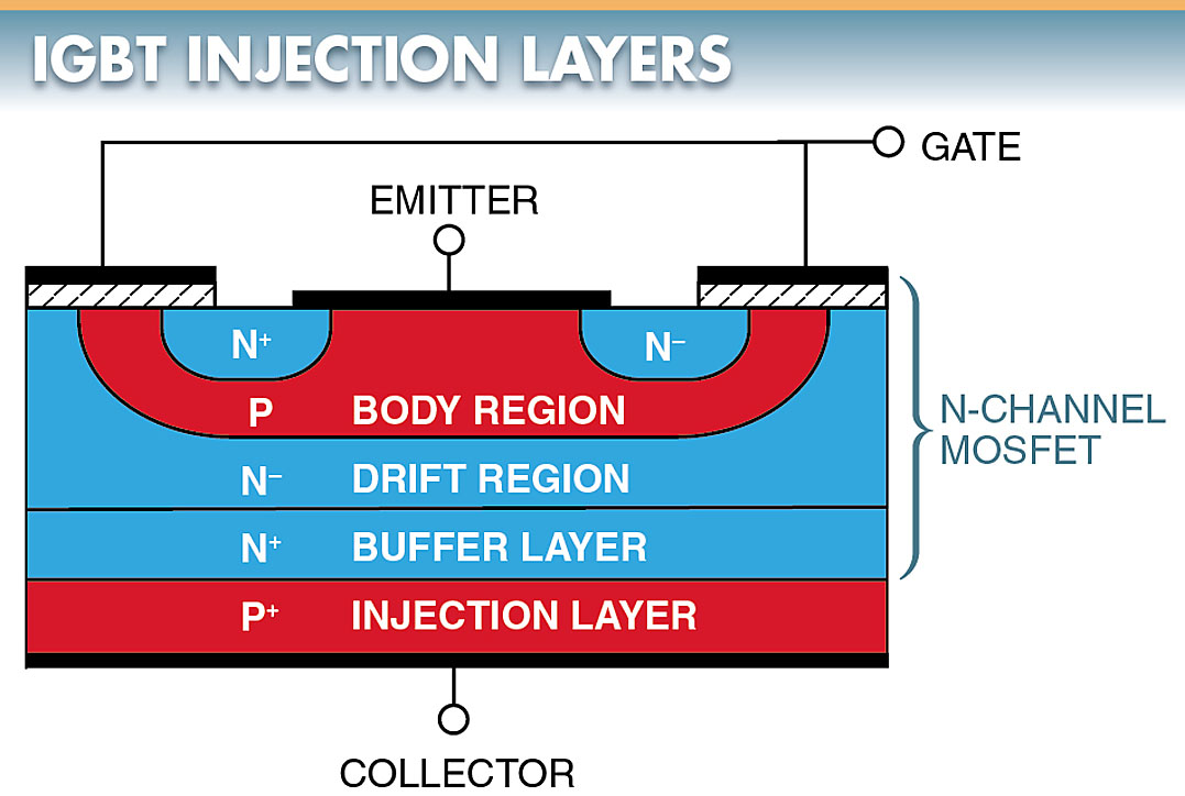
Figure 2. The main difference between a power MOSFET and an IGBT is the addition of an injection layer in the IGBT.
Insulated Gate Bipolar Transistor Operation
IGBTs are fast switching devices. IGBT operations consist of blocking, ON/OFF state, and latch-up operations. The safe operating area (SOA) of an IGBT protects against inductive shutoff.
The two IGBT configurations include the punch-through (PT) and non-punch-through (NPT) configurations.
Blocking Operation
The ON/OFF state of an IGBT is determined by the gate voltage.
If the voltage applied to the gate contact, with respect to the emitter, is less than the threshold voltage, then no MOSFET inversion layer is created and the device is turned off. When this is the case, any applied forward voltage should fall across the reverse-biased junction. The only current flow should be a small leakage current.
The forward breakdown voltage is, therefore, determined by the breakdown voltage of the junction. This is important for power devices with large voltages and currents.
The breakdown voltage of the junction is dependent on the doping. A lower doping ratio results in a wider depletion region and a lower maximum electric field in the depletion region, which is why the drift region (N–) is doped much lighter than the body region.
The buffer layer (N+) is present to prevent the depletion region from extending into the bipolar collector. The benefit of this buffer layer is that it allows the thickness of the drift region to be reduced, thus reducing ON-state losses.
ON-State Operation
The ON-state of the IGBT is achieved by increasing the gate voltage so that it is greater than the threshold voltage. That increase in voltage results in an inversion layer forming under the gate, which provides a channel linking the source to the drift region of the IGBT. Electrons are then injected from the source into the drift region. At the same time, holes are injected into the drift region.
This injection causes conductivity of the drift region, where both the electron and hole densities are higher than the original N– doping. This conductivity gives the IGBT its low ON-state voltage. This is possible because of the reduced resistance of the drift region.
Some of the injected holes should recombine in the drift region. Others may cross the region by drift and diffusion and reach the junction of the body region where they are collected.
OFF-State Operation
Either the gate must be shorted to the emitter or a negative bias must be applied to the gate.
When the gate voltage falls below the threshold voltage, the inversion layer cannot be maintained, and the supply of electrons into the drift region is blocked. At this point, the shutoff process begins.
The shutoff process cannot be completed as quickly as desired due to the high concentration of minority carriers injected into the drift region during forward conduction. The collector current rapidly decreases due to the termination of the electron current through the channel. Then the collector current is reduced as the minority carriers recombine.
Latch-Up Operation
During ON-state operation, paths for current to flow in an IGBT allow holes to be injected into the drift region from the collector (P+).
Parts of the holes disappear by recombination with electrons from the MOSFET channel. Other parts of the holes are attracted to the vicinity of the injection layer by the negative charge of electrons. These holes cross the body region and develop a voltage drop in the resistance of the body.
Once in a latch-up condition, the MOSFET gate has no control over the collector current. The only way to shut off the IGBT is to shut off the current, just as for a conventional SCR.
Note: If latch-up is not terminated quickly, the IGBT may be destroyed by the excessive power dissipation.
IGBT Safe Operating Area
The safe operating area (SOA) is the current-voltage limit in which a power switching device like an IGBT can be operated without being destroyed. The area is defined by the maximum collector-emitter voltage (VCE) and collector current (IC) the IGBT operation must control to protect the IGBT from damage.
The types of SOAs for IGBTs are the forward-biased safe operating area (FBSOA), reverse-biased safe operating area (RBSOA), and short-circuit safe operating area (SCSOA). The two primary conditions that could affect the SOA of an IGBT are operation during a short circuit and inductive shutoff.
Protection must be in place when switching inductive loads. This can be done by the use of regular diodes, Zener diodes, or resistors. The method used depends on the application. IGBTs often need this type of protection from inductive loads to prevent inductive shutoff.
TECH FACT
IGBTs that are used in variable frequency drives as the motor switching devices will sometimes fail. Failure can be reduced by using line and load reactors, limiting the distance between drive and motor, allowing enough open space for drive cooling, increasing motor acceleration/deceleration times, lowering the PWM frequency setting, ensuring proper grounding, and not loading the drive more than 80% of its rating.
PT and NPT Configurations
The two types of structures used for Insulated Gate Bipolar Transistor construction are the punch-through (PT) structure and the non-punch-through (NPT) structure.
An IGBT is called a PT IGBT when there is a buffer layer (N+) between the injection layer (P+) and the drift region (N–). Otherwise, it is called an NPT IGBT.
The buffer layer improves shutoff speed by reducing the minority-carrier injection quantity and raising the recombination rate during the switching transition.
The PT IGBT has similar characteristics as the NPT IGBT for switching speed and forward voltage drop. Currently, most commercialized IGBTs are PT IGBTs.
Insulated Gate Bipolar Transistor (IGBT) Key Takeaways
Understanding the operation, characteristics, and configurations of IGBTs is crucial for their effective use in high-power and high-voltage applications. Their unique combination of MOSFET control and bipolar transistor switching makes them ideal for systems requiring efficient, fast, and reliable power handling, such as motor drives, renewable energy systems, electric vehicles, and industrial inverters. The distinction between PT and NPT structures, along with safe operating area considerations, directly impacts the performance and longevity of IGBTs in these demanding environments. Proper application and protection strategies are essential to maximize their benefits and ensure system stability and efficiency.