The article explains the fundamental theory of PN junction in semiconductor diodes, focusing on the formation of the depletion region, diffusion and drift currents, and how the junction behaves under forward and reverse bias. It also outlines the diode’s I-V characteristics, including the effects of Zener and avalanche breakdown in reverse-biased conditions.
A simple section of n- or p-type material is not particularly useful for the construction of electronic circuits. However, when sections of n- and p-type material are brought in contact to form a PN junction, a diode is formed. Diodes have a number of interesting and useful properties that are due entirely to the nature of the PN junction.
Figure 1 depicts an idealized PN junction. The difference in concentrations of free electrons in the n-type material compared to the p-type material results in a diffusion of free electrons from right to left across the junction. Likewise, the difference in concentration of holes on either side of the junction results in diffusion of holes from left to right across the junction.
In both cases, the diffusion current Id is directed left to right because a positive current is defined as either positive holes moving left to right or negative free electrons moving right to left.
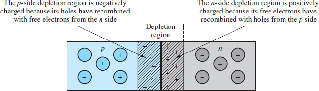
Figure 1 A PN junction
As free electrons leave the n-type material and enter the p-type material they tend to recombine with holes. Likewise, as holes leave the p-type material and enter the n-type material they tend to recombine with free electrons.
Once free electrons and holes recombine, they are no longer mobile, but held in place in the material lattice by covalent bonds.
At first, most of the recombination occur close to the junction. However, as time passes, more and more of the mobile charges near the junction have recombined such that diffusing mobile charges must travel further from the junction to encounter a partner with which to recombine. Thus, this diffusion process results in recombination on both sides of the junction and, as the process continues, an expanding depletion region wherein virtually no mobile charge carriers remain. This region is electrically charged because mobile charge carriers that have recombined to form the region have no electrical counterpart in the lattice where they have become fixed. In Figure 1 this result is depicted by the negatively charged p-type region to the left of the junction and the positively charged n-type region to the right of the junction.
Once the depletion region begins to form, the resulting net charge separation produces an electric field pointing from the positively charged n-type to the negatively charged p-type portions of the depletion region. This electric field slows the ongoing diffusion of majority charge carriers by establishing a potential barrier or contact potential across the depletion region. This potential depends upon the semiconductor material (about 0.6 to 0.7 V for silicon) and is also known as the offset voltage Vγ.
In addition to the diffusion current associated with majority charge carriers, an oppositely directed drift current IS associated with minority charge carriers is established across the depletion region.
Specifically, free electrons and holes are thermally generated in the p- and n-type materials, respectively. Any of these minority carriers that manage to reach the depletion region are swept across it by the electric field.
Note that both components of the drift current contribute to a positive current from right to left because a positive current is defined as either positive hole moving right to left or negative free electrons moving left to right.
Figure 2 depicts the presence of both a diffusion current and drift current across the depletion region. Its equilibrium width is reached when the average net drift current exactly offsets the average net diffusion current.
Recall that the magnitude of the diffusion current is largely determined by the concentration of the donor and acceptor elements while the magnitude of the drift current is highly temperature dependent. Thus, the equilibrium width of the depletion region depends upon both temperature and the doping process.
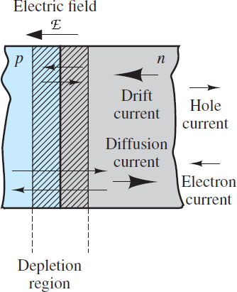
Figure 2 Drift and diffusion currents in a PN junction
Now consider the case shown in Figure 3(a) where a battery has been connected across a PN junction in the reverse-biased direction. Assume that suitable contacts between the battery and the p- and n-type materials are established.
The reverse-bias orientation of the battery widens the depletion region and increases the potential barrier across it such that the majority carrier diffusion current decreases.
On the other hand, the minority carrier drift current increases such that there is now a small (on the order of nano-amperes) non-zero current I0 directed from the n- to p-type region. I0 is small because it is comprised of minority carriers. Thus, when reverse-biased, the diode current iD is:
${{i}_{D}}=-{{I}_{0}}={{I}_{S}}$ Reverse-based diode current
Where IS is known as the reverse saturation current.
When the PN junction is forward-biased as in Figure 3(b), the depletion region is narrowed and the potential barrier across it is lowered such that the majority carrier diffusion current increases. As the forward-biased diode voltage vD is increased the diffusion current Id increases exponentially:
\[{{I}_{d}}={{I}_{0}}{{e}^{{{q}_{e}}{{v}_{D}}/kT}}={{I}_{0}}{{e}^{{{v}_{D}}/{{V}_{T}}}}\begin{matrix}{} & {} & (1) \\\end{matrix}\]
Where qe = 1.6 × 10⁻¹⁹ C is the elementary charge, T is the material temperature (in K), and VT = kT/qe is the thermal voltage. At room temperature, VT ≈ 25 mV. The net diode current under forward bias is:
\[{{i}_{D}}={{I}_{d}}-{{I}_{0}}={{I}_{0}}({{e}^{{{v}_{D}}/{{V}_{T}}}}-1)\begin{matrix}{} & Diode\text{ }Equation & (2) \\\end{matrix}\]
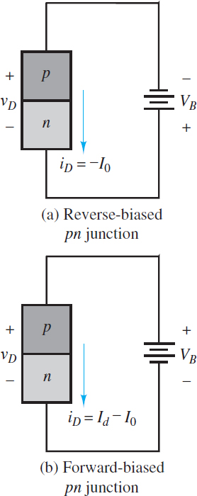
Figure 3 Forward- and reverse-biased PN junctions
Figure 4 depicts the diode i-v characteristic described by the diode equation for a fairly typical silicon diode for vD > 0. Since I0 is typically very small (10−9 to 10−15 A), the diode equation is often approximated by:
\[{{i}_{D}}={{I}_{0}}{{e}^{{{v}_{D}}/{{V}_{T}}}}\begin{matrix}{} & {} & (3) \\\end{matrix}\]
This expression is a good approximation for a silicon diode at room temperature when vD is greater than a few tenths of a volt.
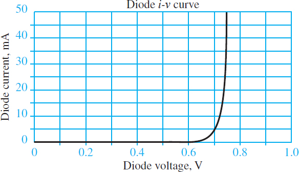
Figure 4 Typical diode i-v characteristic curve
The ability of the PN junction to conduct significant current only in the forward-biased direction allows it to function in electric circuits much like a check valve functions in mechanical circuits. A generic PN junction and the diode circuit symbol are shown in Figure 5. Notice that the triangle shape suggests the direction of forward-biased current. Positive current iD passes from the anode to the cathode, where the term cathode always refers to the source of electrons (negative charge carriers) whether used in reference to a diode or battery.
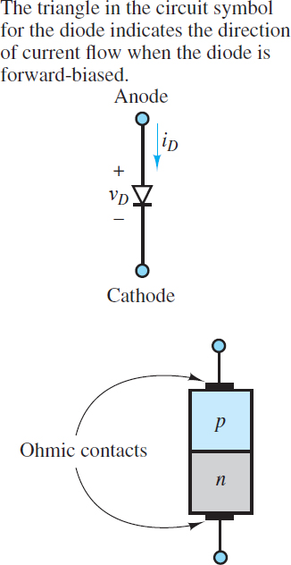
Figure 5 Diode circuit symbol
Figure 6 shows the complete i-v characteristic of a diode. Note that the diode current is approximately zero when vD < 0 unless vD is sufficiently large and negative (reverse-biased) such that reverse breakdown occurs. When v D < − VZ, the diode conducts current in the reverse-biased direction. Two effects contribute to this reverse-biased current: the Zener effect and avalanche breakdown. In silicon diodes, the Zener effect tends to dominate when VZ < 5.6 V while avalanche breakdown tends to dominate at larger, more negative diode voltages.
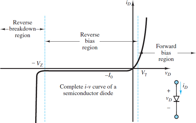
Figure 6 The diode i-v characteristic
The root causes of these two effects, while similar, are not the same. The Zener effect is significant when the depletion region is designed to be heavily doped but very thin such that for a given potential difference vD, the electric field is large enough to sever covalent bonds in the depletion region and generate pairs of free electrons and holes, which are then swept away by the electric field, thus creating a current.
Avalanche breakdown occurs when the potential difference vD is large enough that the kinetic energy of minority charge carriers is sufficient to break covalent bonds during collisions. These collisions may liberate free electrons and holes, which, again, are swept away by the electric field.
The process by which energy is imparted to new charge carriers is called impact ionization. These new charge carriers may also have enough energy to energize other low-energy electrons, such that a sufficiently large reverse-biased diode voltage may initiate an avalanche of liberated charge carriers.
In Zener breakdown the high concentration of charge carriers provides the means for a substantial reverse-biased current to be sustained, at a nearly constant reverse-biased voltage, the Zener voltage VZ. This effect is very useful in applications where one would like to regulate (hold constant) the voltage across a load.
It should also be noted that a typical silicon diode is not designed for use in reverse breakdown, where even a modest current at a large VZ will likely generate more power than the diode can dissipate through heat transfer. The result could be a melted or burned diode!
PN Junction Theory for Semiconductor Diodes Key Takeaways
Understanding the behavior of PN junctions is essential because they form the core of semiconductor devices like diodes, transistors, and voltage regulators. The concepts of depletion region formation, drift and diffusion currents, and biasing conditions directly influence how these devices operate in real-world electronic circuits. The ability of a diode to allow current flow in only one direction (forward bias) and block it in the reverse, except during controlled breakdowns (Zener or avalanche), makes it vital in applications such as rectification, signal demodulation, switching, and voltage regulation. Without the unique electrical properties offered by the PN junction, modern electronic systems—ranging from simple chargers to advanced communication devices—would not be possible.