Photoelectric devices typically contain solid-state output switches. A solid-state switch has no moving parts (contacts). A solid-state switch uses a triac, SCR, NPN (current sink) transistor, or PNP (current source) transistor output to perform the switching function. See Figure 1.
The triac output is used for switching AC loads. The SCR output is used for switching high-power DC loads. The current sink and current source transistor outputs are used for switching low-power DC loads. Solid-state switches include normally open (NO), normally closed (NC), or combination switching outputs.
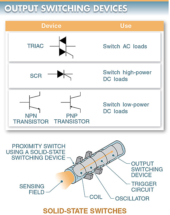
Figure 1. A solid-state switch uses a triac, SCR, NPN (cur- rent sink) transistor, or PNP (current source) transistor output to perform the switching function.
Tech Fact
Common photoelectric or proximity switch cylindrical housings are available in 5mm, 8mm, 12mm, 18mm, 25mm, and 30mm sizes (though 18 mm is the most common size). The millimeter (mm) rating refers to the diameter of the sensor’s heat-sensing head. The larger the diameter of the sensing head, the farther the sensing distance.
- You May Also Read: Transistor Working Principle
Solid-state devices are usually connected (interfaced) through the use of electrical devices. They can also be interfaced through light-driven systems. Once light rays have passed through the optical fiber, they must be detected and converted back into electrical signals.
The detection and conversion are accomplished with light-activated devices such as PIN photodiodes, phototransistors, light-activated SCRs, and phototriacs. The light source must be properly matched to the light-activated device to operate effectively. The source must also be of sufficient intensity to drive the light-activated device.
PIN Photodiodes
A PIN photodiode is a diode with a large intrinsic region sandwiched between P-type and N-type regions. PIN stands for P-type material, insulator, and N-type material. See Figure 2.
The operation of a PIN photodiode is based on the principle that light radiation, when exposed to a PN junction, momentarily disturbs the structure of the PN junction. The disturbance is due to a hole created when a high-energy photon strikes the PN junction and causes an electron to be ejected from the junction. Thus, light creates electron-hole pairs that act as current carriers. PIN photodiodes are used in gas detectors, spectrometers, and gas analyzers.
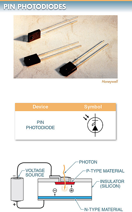
Figure 2. A PIN photodiode is a diode with a large intrinsic region sandwiched between P-type and N-type regions.
Phototransistors
A phototransistor is a device that combines the effect of a photodiode and the switching capability of a transistor.
The symbol for a phototransistor is similar to the symbol for a standard transistor except with the addition of two arrows that represent a light source pointing into the transistor. See Figure 3.
A phototransistor, when connected in a circuit, is placed in series with the bias voltage so that it is forward biased.
In a two-lead phototransistor, the base lead is replaced by a clear covering that allows light to fall on the base region. Light falling on the base region causes current to flow between the emitter and collector. The collector-base junction is enlarged and works as a reverse-biased photodiode controlling the phototransistor.
The phototransistor conducts more or less current, depending on the light intensity. If the light intensity increases, resistance decreases, and more emitter-to-base current is created. Although the base current is relatively small, its amplifying capability is used to control the large emitter-to-collector current.
The collector current depends on the light intensity and the DC current gain of the phototransistor. In the darkness, the phototransistor is switched off with the remaining leakage current (collector dark current).
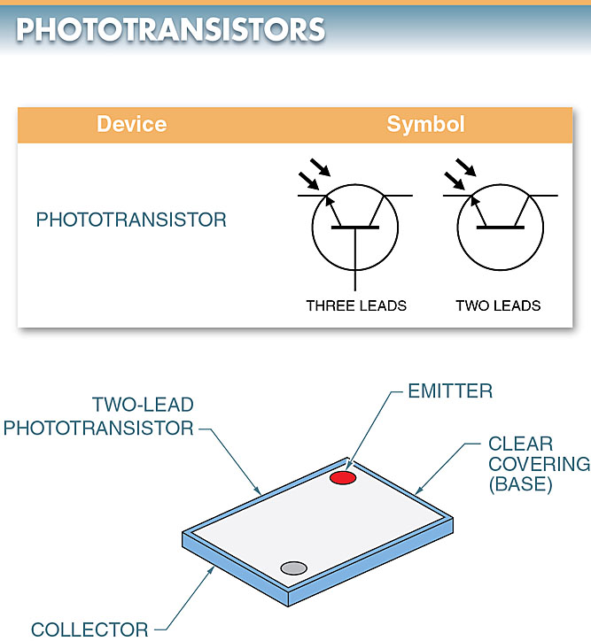
Figure 3. A phototransistor is a device that combines the effect of a photodiode and the switching capability of a transistor.
Light-Activated SCRs
A light‐activated SCR (LASCR) is an SCR that is activated by light. The symbol of a LASCR is identical to the symbol of a regular SCR with one difference. The only difference is that arrows are added in the LASCR symbol to indicate a light-sensitive device. See Figure 4.
Similar to a photodiode, a very low level of current is in a LASCR. Even the largest LASCRs are limited to a maximum of a few amps. When larger current requirements are necessary, a LASCR can be used as a trigger circuit for a standard high-power switching SCR.
The primary advantage of a LASCR over an SCR is its ability to provide isolation. Because the LASCR is triggered by light, it provides complete isolation between the input signal and the output load current.
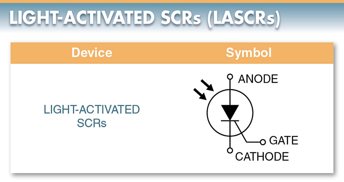
Figure 4. A light-activated SCR (LASCR) is an SCR that is activated by light.
Phototriacs
A phototriac is a triac that is activated by light. See Figure 5.
The gate of a phototriac is light sensitive. It triggers the triac at a specified light intensity. In the darkness, the triac is not triggered. The remaining leakage current is referred to as peak blocking current. A phototriac is bilateral and designed to switch AC signals.
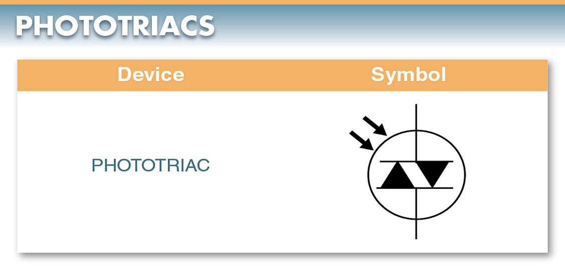
Figure 5. A phototriac is a triac that is activated by light.
Light-Emitting Diodes
A light‐emitting diode (LED) is a semiconductor diode that produces light when current flows through it.
As electrons move across the depletion region, they give up extra kinetic energy. The extra energy is converted to light. An electron must acquire additional energy to get through the depletion region. This additional energy comes from the positive field of the anode. If the positive field is not strong, the electron will not get through the depletion region and no light will be emitted. See Figure 6.
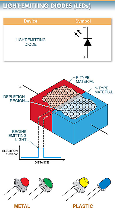
Figure 6. A light-emitting diode (LED) is a semiconductor diode that produces light when current flows through it.
For a standard silicon diode, a minimum of 0.6 V must be present before the diode conducts. For a germanium diode, 0.3 V must be present before the diode conducts. Most LED manufacturers make a larger depletion region that requires 1.5 V for the electrons to get across.
LED Construction
LED manufacturers normally use a combination of gallium and arsenic with silicon or germanium to construct LEDs. By adding other impurities to the base semiconductor and adjusting them, the manufacturers can produce different wavelengths of light. LEDs are capable of producing infrared light. Infrared light is light that is not visible to the human eye. LEDs may emit a visible red or green light. Colored plastic lenses are available if different colors are desired.
As with standard semiconductor diodes, there is a method for determining which end of an LED is the anode and which end is the cathode. The cathode lead is identified by the flat side of the device or a notch that may have been cut into the ridge.
A colored plastic lens focuses the light produced at the junction of the LED. Without the lens, the small amount of light produced at the junction is diffused and becomes virtually unusable as a light source. The size and shape of the LED package determine how it is positioned for proper viewing.
The schematic symbol for an LED is exactly like that of a photodiode, but the arrows point away from the diode. The LED is forward biased and a current-limiting resistor is normally present to protect the LED from excessive current.
Laser Diodes
A laser diode is a diode similar to an LED but with an optical cavity that is required for lasing production (emitting coherent light). The optical cavity is formed by coating opposite sides of a chip to create two highly reflective surfaces. See Figure 7.
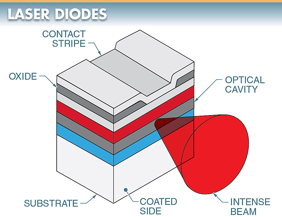
Figure 7. A laser diode is similar to an LED but with an optical cavity that is required for lasing production (emitting coherent light).
Optocouplers
An optocoupler is an electrically isolated device that consists of an IRED as the input stage and an NPN phototransistor as the output stage. An optocoupler is normally constructed as a dual inline package. See Figure 8.
An optocoupler uses a glass dielectric sandwich to separate input from the output. The coupling medium between the LED and sensor are the transmitting glass. This provides one-way transfer of electrical signals from the LED to the photodetector (phototransistor) without an electrical connection between the circuitry containing the devices.
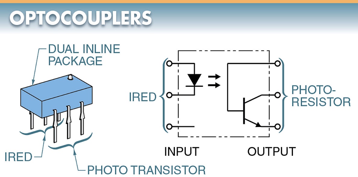
Figure 8. An optocoupler consists of an IRED as the input stage and an NPN phototransistor as the output stage.
Input and output devices are always spectrally matched by their wavelengths for maximum transfer characteristics. The signal cannot go back in the opposite direction because the emitters and detectors cannot reverse their operating functions.
