
An operational amplifier (op-amp) is an integrated circuit (IC) that contains a large number of microscopic electrical and electronic components integrated on a single silicon wafer. An op-amp can be used in conjunction with other common components to create circuits that perform amplification and filtering, as well as mathematical operations, such as addition, subtraction, multiplication, differentiation, and integration, on electrical signals.
Op-amps are found in most measurement and instrumentation applications, serving as a versatile building block for many applications.
The behavior of an op-amp is well described by fairly simple models, which permit an understanding of its effects and applications without delving into its internal details. Its simplicity and versatility make the op-amp an appealing electronic device with which to begin understanding electronics and integrated circuits.
The lower right portion of Figure 1 shows a standard single op-amp IC chip pin layout. It has two input pins (2 and 3) and one output pin (6). Also notice the two DC power supply pins (4 and 7) that provide external power to the chip and thus enable the op-amp. Operational amplifiers are active devices; that is, they need an external power source to function. Pin 4 is held at a low DC voltage $V_{S}^{-}$, while pin 7 is held at a high DC voltage $V_{S}^{+}$. These two DC voltages are well below and above, respectively, the op-amp’s reference voltage and bound the output of the op-amp.
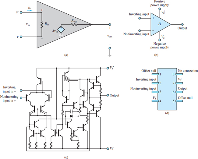
Figure 1(a) Small-signal op-amp model; (b) simplified op-amp circuit symbol; (c) generic op-amp IC schematic; (d) single op-amp IC chip pin layout.
The upper left portion of Figure 1 shows the so-called small-signal, low-frequency model of an op-amp. For this model, the input impedance is Rin and the output impedance is Rout. The op-amp itself is a differential amplifier because its output is a function of the difference between two input voltages, v+ and v–, which are known as the non-inverting and inverting inputs, respectively.
Notice that the value of the internal dependent voltage source is A (v+ − v–), where A is the open-loop gain of the op-amp. In a practical op-amp, A is quite large by design, typically on the order of 105 to 107. This large open-loop gain can be exchanged, by design, for a smaller closed-loop gain G to acquire various beneficial characteristics for an amplifier circuit, of which the op-amp is just one component.
The Ideal Op-Amp
Practical op-amps have a large open-loop gain A, as noted above. The input impedance Rin is also large, typically on the order of 106 to 1012 Ω, while the output impedance Rout is small, typically on the order of 100 or 101 Ω.
In the ideal case, the open-loop gain and the input impedance would be infinite, while the output impedance would be zero. When the output impedance is zero, the output voltage of an ideal op-amp is simply:
\[{{v}_{out}}=A({{v}^{+}}-{{v}^{-}})=A\Delta v\begin{matrix}{} & {} & (1) \\\end{matrix}\]
But is this relationship practical when the open-loop gain A approaches infinity? The implication for a practical op-amp is that one of the two following possibilities will hold:
- In the case that Δv ≠ 0, the output voltage saturates near either the positive or negative DC power supply value, $V_{S}^{+}$or$V_{S}^{-}$, as shown in Figure 2. These external DC power supply rails enable a practical op-amp to function but also bound the op-amp output voltage vout. This case applies to all practical applications of an op-amp used in open-loop mode; that is, when there is no feedback from vout to v–.
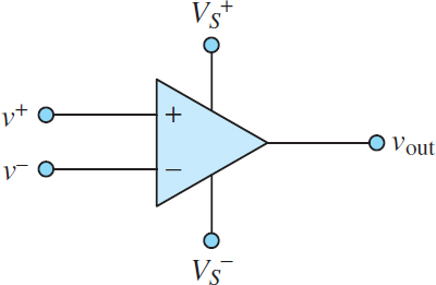
Figure 2 Ideal operational amplifier
- In the case that Δv = 0, the output voltage is not determined by the op-amp itself but by whatever other circuitry is attached to it. When Aβ ≫ 1 the closed-loop gain of an amplifier is approximately equal to 1/β and largely independent of A itself. Thus, this case applies to all practical applications of an op-amp in closed-loop mode; that is, when negative feedback is present from vout to v–.
Notice in Figure 2 that the letter “A” does not appear within the triangle symbol, thus implying that the open-loop gain is infinite. Also implied by the ideal op-amp symbol is that the current into or out of either input terminal is zero. This result is a consequence of the infinite input impedance of an ideal op-amp and is known as the first golden rule of ideal op-amps:
\[\begin{matrix}{{i}^{+}}={{i}^{-}}=0 & First\text{ }golden\text{ }rule & (2) \\\end{matrix}\]
When Aβ ≫ 1 the difference between the two amplifier inputs, us and uf, approaches zero. In the context of ideal op-amps, where A → ∞, the difference between the two amplifier inputs, v+ and v–, will be zero exactly as long as there is a feedback path from vout to v–.
\[\begin{matrix}{{v}^{+}}={{v}^{-}} & \text{Second golden }rule;negative\text{ }feedback\text{ }required & (3) \\\end{matrix}\]
The Golden Rules of Ideal Op-Amps:
i+ = i– = 0.
v+ = v– (when negative feedback is present).
Amplifier Archetypes
There are three fundamental amplifiers that utilize the operational amplifier and employ negative feedback. They are:
- The inverting amplifier.
- The non-inverting amplifier.
- The isolation buffer (or voltage follower).
These archetypes have many important applications and are the building blocks for other important amplifiers.
Understanding and recognizing these archetypes is an essential first step in the study of amplifiers based upon the op-amp. It is worth emphasizing that the op-amp is rarely used as a stand-alone amplifier; rather it is used along with other components to form specialized amplifiers.
Inverting Amplifier
Figure 3 shows a basic inverting amplifier circuit. The name derives from the fact that the input signal vS “sees” the inverting terminal (−) and that, as is shown below, the output signal vo is an inverted (negative) version of the input signal.
The goal of the following analysis is to determine the relationship between the output and the input signals. To begin, assume the op-amp is ideal and apply KCL at the inverting node marked v–.
\[{{i}_{S}}={{i}_{F}}+{{i}_{in}}\begin{matrix}{} & {} & (4) \\\end{matrix}\]
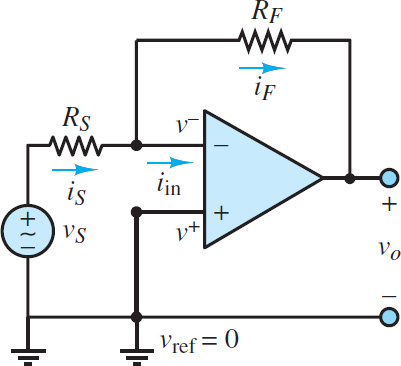
Figure 3 Inverting amplifier
However, the first golden rule of ideal op-amps states that iin = i– = 0. Thus, iS = iF such that RS and RF form a virtual series connection. Ohm’s law can be applied to each resistor to yield:
\[{{i}_{S}}=\frac{{{v}_{S}}-{{v}^{-}}}{{{R}_{S}}}\begin{matrix}{} & \begin{matrix}{{i}_{F}}=\frac{{{v}^{-}}-{{v}_{0}}}{{{R}_{F}}} & {} & {} \\\end{matrix} & (5) \\\end{matrix}\]
These expressions can be simplified by noting that v+ = 0 and then applying the second golden rule of ideal op-amps to realize v– = v+ = 0. Thus:
\[\begin{matrix}\begin{align}& {{i}_{S}}={{i}_{F}} \\& or \\& \frac{{{v}_{S}}}{{{R}_{S}}}=\frac{-{{v}_{0}}}{{{R}_{F}}} \\\end{align} & {} & \left( 6 \right) \\\end{matrix}\]
Cross-multiply to find the closed-loop gain G:
\[\begin{matrix}G=\frac{{{v}_{0}}}{{{v}_{S}}}=-\frac{{{R}_{F}}}{{{R}_{S}}} & Inverting\text{ }Amplifier & (7) \\\end{matrix}\]
Note that the magnitude of G can be greater or less than 1.
An alternate approach is to apply voltage division across the virtual series connection of RS and RF.
\[\begin{matrix}\begin{align}& \frac{{{v}_{S}}-{{v}_{0}}}{{{v}_{S}}-0}=-\frac{{{R}_{S}}+{{R}_{F}}}{{{R}_{S}}} \\& or \\& 1-\frac{{{v}_{0}}}{{{v}_{S}}}=1+\frac{{{R}_{F}}}{{{R}_{S}}} \\\end{align} & {} & \left( 8 \right) \\\end{matrix}\]
Subtract 1 from each side of this expression to find the same result as equation 7.
Notice that the closed-loop gain G of an inverting amplifier is determined solely by the choice of resistors. This result was derived for an ideal op-amp.
For a practical op-amp the result is only slightly different as long as the open-loop gain A is large. It is important to remember that this result depends upon both golden rules of ideal op-amps and that, in particular, the second golden rule is valid only when negative feedback is present.
As long as the open-loop gain A is large, the presence of negative feedback from the output to the inverting input drives the voltage difference between the two input terminals to zero.
The input impedance of the inverting amplifier is simply:
\[{{R}_{in}}=\frac{{{v}_{in}}}{{{i}_{in}}}=\frac{{{v}_{S}}+0}{{{i}_{S}}}={{R}_{S}}\begin{matrix}{} & {} & (9) \\\end{matrix}\]
Notice the important role played by the virtual ground at the inverting terminal in making this calculation so easy. This result also reveals a shortcoming of the inverting amplifier. In general, an ideal amplifier would have an infinite input impedance so as to not load the source network. It is tempting to correct this problem by choosing RS to be very large; however, in so doing, the closed-loop gain (equation 7) will be reduced. Thus, it is not possible to design an inverting amplifier to have a large gain and also a large input impedance. Alas, there is no such thing as a free lunch!
Non-Inverting Amplifier
Figure 4 shows a basic non-inverting amplifier circuit. The name derives from the fact that the input signal vS “sees” the non-inverting terminal (+) and that, as is shown below, the output signal vo is a non-inverted (positive) version of the input signal.
The goal of the following analysis is to determine the relationship between the output and the input signals. As was done for the inverting amplifier circuit, assume the op-amp is ideal and apply KCL at the inverting node marked v–.
\[{{i}_{F}}={{i}_{1}}+{{i}_{in}}\begin{matrix}{} & {} & (10) \\\end{matrix}\]
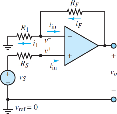
Figure 4 Non-inverting amplifier
However, the first golden rule of ideal op-amps states that iin = i– = i+ = 0. Thus, iF = i1 such that RF and R1 form a virtual series connection. Ohm’s law can be applied to each resistor to yield:
\[\begin{matrix}{{i}_{1}}=\frac{{{v}^{-}}-0}{{{R}_{1}}} & {} & {{i}_{F}}=\frac{{{v}_{out}}-{{v}^{-}}}{{{R}_{F}}} \\or & {} & (11) \\\frac{{{v}^{-}}}{{{R}_{1}}}=\frac{{{v}_{0}}-{{v}^{-}}}{{{R}_{F}}} & {} & {} \\\end{matrix}\]
Since there is negative feedback present, the second golden rule of ideal op-amps can be applied such that v– = v+. Notice that because iin = 0, the voltage drop across RS is zero with the result that v– = v+ = vS. Substitute this result into equation 11 and rearrange terms to yield the closed-loop gain G:
\[\begin{matrix}G=\frac{{{V}_{0}}}{{{v}_{S}}}=1+\frac{{{R}_{F}}}{{{R}_{1}}} & Non-inverting\text{ }amplifier & (12) \\\end{matrix}\]
Note that G ≥ 1.
An alternate approach is to apply voltage division across the virtual series connection of R1 and RF.
\[\frac{{{V}_{0}}-0}{{{v}^{-}}-0}=\frac{{{R}_{1}}+{{R}_{F}}}{{{R}_{1}}}\begin{matrix}{} & {} & (13) \\\end{matrix}\]
Since v– = vS:
\[\frac{{{V}_{0}}}{{{v}_{S}}}=1+\frac{{{R}_{F}}}{{{R}_{1}}}\begin{matrix}{} & {} & (14) \\\end{matrix}\]
Which is the same result as that found in equation 12.
Notice that the closed-loop gain G of a non-inverting amplifier is also determined solely by the choice of resistors. This result was derived for an ideal op-amp.
For a practical op-amp the result is only slightly different as long as the open-loop gain A is large. It is important to remember that this result depended upon both golden rules of ideal op-amps and that, in particular, the second golden rule is valid only when negative feedback is present.
As long as the open-loop gain A is large, the presence of negative feedback from the output to the inverting input drives the voltage difference between the two input terminals to zero.
The input impedance of the non-inverting amplifier is simply:
\[{{R}_{in}}=\frac{{{v}_{in}}}{{{i}_{in}}}=\frac{{{v}_{S}}-0}{{{i}_{in}}}\to \infty \begin{matrix}{} & {} & (15) \\\end{matrix}\]
In practice, the input impedance of a non-inverting amplifier is very large due to the very large input impedance of the op-amp, which limits iin to very small values.
Notice that the closed-loop gain of the non-inverting amplifier is independent of its input impedance. Thus, the non-inverting amplifier does not suffer from a trade-off between gain and input impedance, as does the inverting amplifier.
However, the gain of a non-inverting amplifier is limited to values greater than one, whereas the gain of the inverting amplifier can take on any value.
Isolation Buffer or Voltage Follower
Figure 5 shows an isolation buffer, which is also known as a voltage follower. Notice that the input signal vS “sees” the non-inverting terminal (+) such that the output signal vo should be a non-inverted (positive) version of vS.
The analysis of this circuit is as simple as the circuit itself. Assume that the op-amp is ideal. Since negative feedback is present, both golden rules are valid. That is:
\[{{i}^{+}}={{i}^{-}}=0\begin{matrix}{} & and\begin{matrix}{} & {{v}^{+}}={{v}^{-}}\begin{matrix}{} & {} & (16) \\\end{matrix} \\\end{matrix} \\\end{matrix}\]
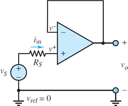
Figure 5 Isolation Buffer or Voltage Follower
By observation, v+ = vS and v– = vout with the result that the closed-loop gain G is:
\[G=\frac{{{v}_{0}}}{{{v}_{S}}}=1\begin{matrix}{} & Isolation\text{ }Buffer & (17) \\\end{matrix}\]
The reason this circuit is called a voltage follower should now be obvious; the output voltage vo “follows” (equals) the input voltage vS. On the other hand, the reason this circuit is also known as an isolation buffer is not obvious. However, since i+ = 0, the ideal op-amp is said to possess an infinite input resistance or input impedance such that the voltage source experiences no loading from the op-amp. Yet the circuit still reproduces vS at the output.
Any loading effects at the output are experienced by the op-amp rather than the voltage source, such that the source is isolated or buffered from the output.
The input impedance of an isolation buffer is simply:
\[{{R}_{in}}=\frac{{{v}_{in}}}{{{i}_{in}}}=\frac{{{v}_{S}}-0}{{{i}_{in}}}\to \infty \begin{matrix}{} & {} & (18) \\\end{matrix}\]
In practice, the input impedance of an isolation buffer is very large due to the very large input impedance of the op-amp, which limits iin to very small values. The closed-loop gain is fixed at unity as long as the open-loop gain A is large such that v– will be driven to v+ by negative feedback.
