A Bipolar Junction Transistor (BJT) is formed by joining three sections of alternating p- and n-type material. An NPN transistor is a BJT with a thin, lightly doped p-type base region sandwiched between a heavily doped n-type emitter region and a large, lightly doped n-type collector region.
The Bipolar Junction Transistor (BJT) counterpart to the NPN is the PNP transistor, which utilizes the same doping scheme except that the n and p regions are swapped with respect to the NPN. In both of these BJT types, the heavily doped emitter region is often labeled n+ or p+ to distinguish it from the lightly doped collector.
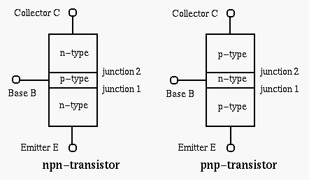
Figure 1 illustrates the construction, symbols, and nomenclature for the two types of Bipolar Junction Transistor (BJTs). Notice that there are the two PN junctions in a BJT: the emitter-base junction (EBJ) and the collector-base junction (CBJ). The operating mode of a BJT depends upon whether these junctions are reverse- or forward-biased, as indicated in Table 1.
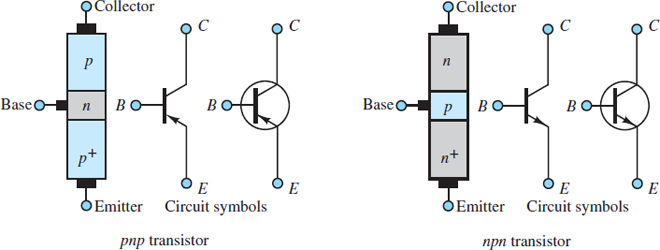
Figure 1 Bipolar junction transistors (BJT)
Table 1 BJT operating modes
| Mode | EBJ | CBJ | Application |
| Cutoff | Reverse-biased | Reverse-biased | Open switch |
| Active | Forward-biased | Reverse-biased | Amplifier |
| Saturation | Forward-biased | Forward-biased | Closed switch |
Although the construction of a Bipolar Junction Transistor (BJT) results in two opposing PN junctions, it is important to avoid modeling a BJT as two identical but opposing diodes. The EBJ always behaves as a true diode; however, because of the thin base region and the lightly doped collector region, the CBJ does not.
Figure 2 depicts the basic geometry of a cross section of a Bipolar Junction Transistor (BJT). The base region is shown much thicker (compared to the emitter and collector) for the sake of clarity. There are two key points to note from the figure: (1) the base is a very thin envelope around the emitter, and (2) the collector is much larger than the emitter and the base because it envelopes both and is itself relatively thick compared to the emitter. The result of this geometry is that the collector can receive large numbers of mobile charge carriers without any significant impact upon its density of charge carriers.
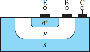
Figure 2 Cross section of an NPN transistor. Notice that the collector is much larger and much more lightly doped than the emitter. However, the base is, in fact, very thin compared to the emitter and collector.
Cutoff Mode (EBJ Reverse-biased; CBJ Reverse-biased)
When both PN junctions are reverse-biased, no current is present across either junction and the path from collector to emitter can be approximated as an open-circuit. In fact, small reverse currents due to minority carriers are present across the junctions, but for most practical applications these reverse currents are negligible.
In silicon-based Bipolar Junction Transistor (BJTs), the offset voltage for the EBJ is the same 0.6 V presented in Chapter 9 for single silicon diodes. Thus, in cutoff mode, when vBE < 0.6 V, the transistor acts as a switch in its off (open-circuit) condition.
Active Mode (EBJ Forward-biased; CBJ Reverse-biased)
Figure 3 shows a Norton source connected across the base and emitter terminals of an NPN transistor and the resulting i-v characteristic of its EBJ. Notice that iB ≈ 0 when vBE ≤ 0.6 V, which is cutoff mode. However, when the EBJ is forward-biased such that vBE ≥ 0.6 V, current is conducted as in a typical diode.
Majority carriers in the emitter and base drift across the EBJ under the influence of the forward-bias voltage in excess of the potential barrier of the depletion region. However, since the emitter is heavily doped while the base is lightly doped, the current IE across the EBJ is dominated by the majority carriers from the emitter.
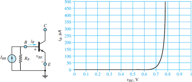
Figure 3 The i-v characteristic of the emitter-base junction of a typical NPN transistor
The i-v characteristics of the EBJ for NPN and PNP transistors are identical except that the abscissas are vBE and vEB, respectively.
The discussion below is based upon the behavior of an NPN transistor; however, the behavior of a PNP transistor is completely analogous to that of an NPN transistor, except that positive and negative charge carriers are interchanged and the EBJ is forward-biased from emitter to base rather than from base to emitter.
The behavior of a PNP transistor is completely analogous to that of an NPN transistor, except that positive and negative charge carriers are interchanged and the EBJ is forward-biased from emitter to base rather than from base to emitter.
For an NPN Bipolar Junction Transistor (BJT), the majority carriers in the emitter are electrons while the majority carriers in the base are holes, as indicated in Figure 4. Some of these electrons recombine with holes in the base; however, since the base is lightly doped, most of these electrons remain mobile minority carriers in the p-type base. As these mobile electrons cross the EBJ, their growing concentration in the base causes them to diffuse toward the CBJ. The equilibrium concentration of these mobile electrons throughout the base region is a maximum at the EBJ and is given by:
\[{{({{n}_{p}})}_{\max }}={{({{n}_{p}})}_{o}}({{e}^{{{v}_{BE}}/{{V}_{T}}}}-1)\begin{matrix}{} & {} & (1) \\\end{matrix}\]
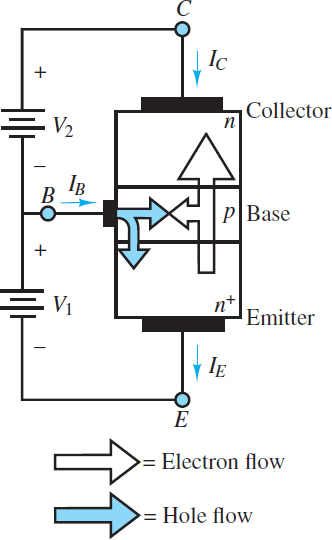
Figure 4 Flow of emitter electrons into the collector in an NPN transistor
Where vBE is the forward-bias voltage from base to emitter and (np)o is the thermal equilibrium concentration of electrons in the base. Since the base is very thin, the equilibrium concentration gradient across the base is nearly linear, as depicted in Figure 5, such that the electron diffusion rate from the EBJ to the CBJ can be approximated as:
\[\frac{A{{q}_{e}}{{D}_{n}}{{({{n}_{p}})}_{\max }}}{W}\begin{matrix}{} & {} & (2) \\\end{matrix}\]
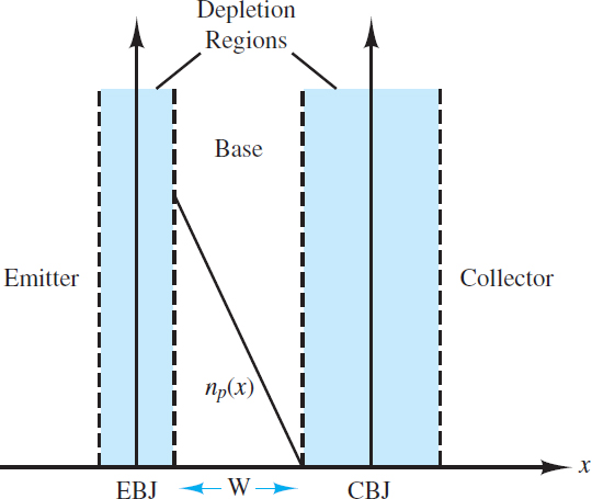
Figure 5 Equilibrium concentration gradient of free electrons in the p-type base of a forward-biased NPN transistor.
Where A is the cross-sectional area of the EBJ, W is the width of the base (not including the width of the two bounding depletion regions), and Dn is the diffusivity of electrons in the base.
It is important to note that this electron diffusion rate is temperature dependent and that it represents a diffusion current directed from the CBJ to the EBJ because of the convention that the direction of positive current is the direction of flow of positive charge carriers. Once these diffusing electrons reach the CBJ they are swept into the collector by the reverse-bias voltage across the CBJ. Thus, the collector current iC is:
\[\begin{matrix}{{i}_{C}}=\frac{A{{q}_{e}}{{D}_{n}}{{({{n}_{p}})}_{0}}}{W}({{e}^{{{v}_{BE}}//{{V}_{T}}}}-1) & {} & {} \\=\frac{A{{q}_{e}}{{D}_{n}}{{n}^{2}}_{i}}{W{{N}_{A}}}({{e}^{{{v}_{BE}}//{{V}_{T}}}}-1) & {} & (3) \\={{I}_{S}}({{e}^{{{v}_{BE}}//{{V}_{T}}}}-1) & {} & {} \\\end{matrix}\]
Where NA is the doping concentration of holes in the base and IS is known as the scale current because it scales with the cross-sectional area A of the EBJ. Typical values of IS range from 10−12 A to 10−15 A.
The base current iB (from base to emitter) is comprised of those majority carriers in the base (e.g., holes for an NPN transistor) that traverse the EBJ. Some of these carriers recombine with the majority carriers in the emitter (e.g., electrons for an NPN transistor); however, those majority carriers lost to recombination are replaced by additional majority carriers supplied by V1. Because the concentration of these majority carriers is proportional to ${{e}^{{}^{{{v}_{BE}}}/{}_{{{V}_{T}}}}}-1$, the base current is proportional to the collector current iC such that:
\[{{i}_{B}}=\frac{{{i}_{C}}}{\beta }=\frac{{{i}_{C}}}{{{h}_{FE}}}\begin{matrix}{} & {} & (4) \\\end{matrix}\]
Where β is known as the forward common-emitter current gain with typical values ranging from 20 to 200. Although β can vary significantly from one transistor to another, most practical electronic devices only require that β>> 1.
Figure 6 depicts the flow of charge carriers from emitter to base to collector and from base to emitter, as discussed above, for an NPN transistor. A Bipolar Junction Transistor (BJT) is a bipolar device because its current is comprised of both electrons and holes.
The parameter β is not often found in a data sheet. Instead, the forward DC value of β is listed as hFE, which is the large-signal current gain. A related parameter, hfe, is the small-signal current gain.
Finally, to satisfy KCL, the emitter current iE must be the sum of the collector and base currents and, therefore, must also be proportional to${{e}^{{}^{{{v}_{BE}}}/{}_{{{V}_{T}}}}}$. Thus:
\[\begin{matrix}\begin{align}& {{i}_{E}}={{I}_{ES}}({{e}^{{{v}_{BE}}//{{V}_{T}}}}-1) \\& ={{i}_{C}}+{{i}_{B}}=\frac{\beta +1}{\beta }{{i}_{C}}=\frac{{{i}_{C}}}{\alpha } \\\end{align} & {} & (5) \\\end{matrix}\]
Where IES is the reverse saturation current and α is the common-base current gain with a typical value close to, but not exceeding, 1.
Saturation Mode (EBJ Forward-biased; CBJ Forward-biased)
A Bipolar Junction Transistor (BJT) remains in active mode as long as the CBJ is reverse-biased; that is, as long as V2 > 0, electrons diffusing across the base will be swept away into the collector once they reach the CBJ. However, when the CBJ is forward-biased (V2 < 0), these diffusing electrons are no longer swept away into the collector but instead accumulate at the CBJ such that the concentration of minority carrier electrons there is no longer zero.
The magnitude of this concentration increases as V2 decreases, such that the concentration gradient across the base decreases. The result is that the diffusion of minority carrier electrons across the base decreases; in other words, the collector current iC decreases as the forward bias of the CBJ increases.
It is important to realize that as the concentration gradient across the base decreases and the rate of diffusion across the base decreases, the rate of increase of the concentration near the CBJ slows and the concentration gradient across the base approaches zero asymptotically. This asymptotic process expresses itself as an upper limit on the forward-bias voltage across the CBJ.
Figure 7 defines three voltages across the terminals of an NPN transistor. In saturation, the action of the transistor limits vCB such that vCE is always positive, although small, with a typical value of 0.2 V.
In fact, saturation mode is often best determined by the value of vCE, which has a value of approximately 0.2 V for a silicon-based Bipolar Junction Transistor (BJT).
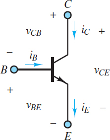
Figure 7 Definition of Bipolar Junction Transistor (BJT) voltages and currents
In saturation, the collector current is no longer proportional to the base current and the collector-emitter voltage VCE for a silicon-based BJT is small (< 0.4 V). An increasing base current drives a BJT further into saturation, and VCE approaches the saturation limit of VCEsat ≈ 0.2 V.
\[{{V}_{CEsat}}\approx 0.2V\begin{matrix}{} & \text{Saturation limit}\begin{matrix}{} & {} & (6) \\\end{matrix} \\\end{matrix}\]
Key Bipolar Junction Transistor (BJT) Characteristics
The voltages and currents shown in Figure 9 for an NPN transistor are related by KCL and KVL.
\[{{v}_{CE}}={{v}_{CB}}+{{v}_{BE}}\begin{matrix}{} & KVL\begin{matrix}{} & {} & (7) \\\end{matrix} \\\end{matrix}\]\[{{i}_{E}}={{i}_{C}}+{{i}_{B}}\begin{matrix}{} & KCL\begin{matrix}{} & {} & (8) \\\end{matrix} \\\end{matrix}\]
The Bipolar Junction Transistor (BJT) currents are temperature dependent because they are proportional to both $n_{i}^{2}$ and${{e}^{{}^{{{v}_{BE}}}/{}_{{{V}_{T}}}}}$. These currents are also proportional to the cross-sectional area A of the EBJ and inversely proportional to the effective width W of the base.
The relationships between these voltages and currents are commonly represented by a graph of iC versus vCE, with iB treated as a parameter. A typical example of such a graph is shown in Figure 8. The operating mode of a BJT is completely specified by these three variables. The three modes of operation are indicated in the figure. Cutoff and saturation modes occur when ic and vCE are very small, respectively.
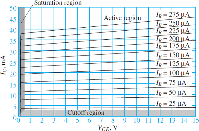
Figure 8 Typical characteristic lines of a Bipolar Junction Transistor (BJT)
For any fixed value of iB, the slope of the transistor characteristic is very small in active mode. In the ideal case, this slope would be zero; however, the effective width of the base decreases with vCE such that the concentration gradient of charge carriers in the base increases and, thus, the collector current increases as well. This increase in iC with vCE is known as the Early effect or base-width modulation.
It is important to realize that the operating values of iB, iC, and vCE, and the operating mode itself, are determined by the external circuitry attached to the Bipolar Junction Transistor (BJT).
It is essential to keep in mind the key characteristics of the cutoff, active, and saturation modes, which are the same for both NPN and PNP transistors, and which are summarized in the box below.
Cutoff mode: Both the EBJ and CBJ are reverse-biased such that all three currents iC, iB, and iE are approximately zero. In cutoff mode, a BJT acts as an open switch between the collector and emitter.
Active mode: The EBJ is forward-biased while the CBJ is reverse-biased. The Bipolar Junction Transistor (BJT) currents are related by:
![]()
In active mode, these currents are largely independent of vCB and the BJT acts as a linear amplifier.
Saturation mode: Both the EBJ and CBJ are forward-biased such that vBE ≈ 0.7 V and vCE≈ 0.2 V. The collector current iC is highly sensitive to small changes in vCE, and, since vCE is small, iC is largely determined by external circuitry attached to the collector terminal. In saturation mode, the BJT approximates a closed switch between the collector and emitter.
Determining the Operating Mode of a Bipolar Junction Transistor (BJT)
A few simple voltage measurements permit a quick determination of the state of a transistor. Consider, for example, an NPN transistor placed in the circuit of Figure 9, where:
![]()
and
![]()
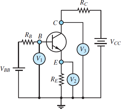
Figure 9 Determination of the operating mode of a Bipolar Junction Transistor (BJT)
Assume that the measured collector, emitter, and base terminal voltages are:
![]()
The method used in determining the state of a transistor is to assume an operating mode and then test the assumption against the known data. It is usually best to first assume cutoff mode and check whether the EBJ is reverse-biased. The voltage across the EBJ is:
![]()
Thus, the EBJ is forward-biased, not reverse-biased, and the transistor is not in cutoff mode.
One can next assume either active or saturation mode and test the assumption. For this example, assume saturation mode and test whether the CBJ is forward-biased. The voltage across the CBJ is:
![]()
Thus, the CBJ is reverse-biased and the transistor is in active mode. The same determination could be made by evaluating the voltage across the collector-emitter terminals.
![]()
The requirement for saturation mode is VCE > 0.4 V, which is clearly not satisfied.
Since the transistor is in active mode, it is possible to calculate the common-emitter current gain β. The base current is:
![]()
The collector current is:
![]()
Thus, the current amplification factor is:
![]()
The operating point of the transistor in the given circuit can be located on a characteristic plot. It is important to note that the operating mode of the transistor is determined by the attached circuitry. In this example, the values of VB, VC, and VE were measured. However, for analytic problems, these values can be calculated using KCL, KVL, Ohm’s law, and the known characteristics of the three possible modes of operation.
